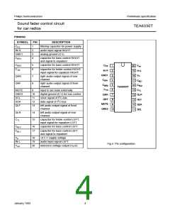
Philips Semiconductors
Preliminary specification
Sound fader control circuit
for car radios
TEA6330T
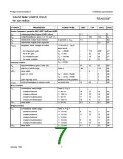
SYMBOL
PARAMETER
CONDITIONS
MIN.
TYP.
MAX.
UNIT
Fader control
G
fader control range
Table 5
0 to
v
−
−30
2
−
dB
dB
dB
step width
1.5
74
2.5
α
mute attenuation
GMB-bit = 1; Table 6
84
−
MUTE
∆V
DC offset output voltage (pins 7, 8, 13,
14)
o
between any adjoining volume step
and any step to mute
G = −66 to 0 dB
−
−
−
−
0.2
2
10
15
10
10
mV
mV
mV
mV
v
G = 0 to +20 dB
v
in any treble and fader position
in any bass position
G = −66 to 0 dB
−
v
G = −66 to 0 dB
−
v
External mute (pin 9)
V
input voltage for MUTE-ON (LOW)
fader is switched into
general mute position
Tables 2 and 5
9
0
3
−
−
−
−
5
−
1.5
V
input voltage for MUTE-OFF (HIGH)
input voltage for MUTE-OFF
input current
V
V
P
pin 9 open-circuit
−
V
I
±10
µA
9
2
I C-bus, SCL and SDA (pins 11 and 12)
V
input voltage HIGH-level
input voltage LOW-level
input current
3
0
−
−
−
−
−
−
V
V
11, 12
P
1.5
±10
0.4
V
I
µA
V
11, 12
V
output voltage at acknowledge (pin 12)
I
= −3 mA
ACK
12
Power-on reset, when reset is active the GMU-bit (general mute) is set and the bus receiver is in reset position
V
supply voltage for start of reset
supply voltage for end of reset
supply voltage for start of reset
increasing voltage
increasing voltage
decreasing voltage
−
−
2.5
6.8
5.8
V
V
V
P
5.2
4.2
6.0
5.0
January 1992
8

 NXP [ NXP ]