Philips Semiconductors
Preliminary specification
Sound fader control circuit
for car radios
TEA6330T
2
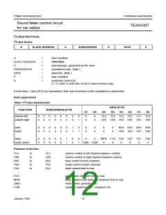
I C-BUS PROTOCOL
2
I C-bus format
S
SLAVE ADDRESS
A
SUBADDRESS
A
DATA
P
S
=
=
=
=
=
=
=
start condition
SLAVE ADDRESS
1000 000X
A
acknowledge, generated by the slave
subaddress byte, Table 1
data byte, Table 1
SUBADDRESS
DATA
P
X
stop condition
read/write control bit
X = 0, order to write (the circuit is slave receiver only)
If more than 1 byte DATA are transmitted, then auto-increment of the subaddress is performed.
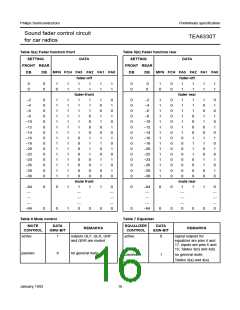
Byte organisation
2
Table 1 I C-bus transmission
DATA BYTE
FUNCTION
volume left
SUBADDRESS BYTE
D7
D6
D5
D4
D3
D2
D1
D0
VL0
0
0
0
0
0
0
0
0
0
0
0
0
0
0
0
1
0
0
0
0
VL5
VL4 VL3 VL2
VL1
volume right
VR5 VR4 VR3 VR2 VR1 VR0
bass
0
0
0
0
0
0
0
0
0
0
0
0
1
1
0
1
0
0
0
0
0
0
0
0
BA3 BA2
TR3 TR2
BA1
TR1
BA0
TR0
treble
fader
0
0
0
0
0
0
0
0
0
0
1
1
0
0
0
1
0
0
MFN FCH FA3 FA2
FA1
0
FA0
0
audio switch
GMU EQN
0
0
0
0
Function of the bits:
VL0
VR0
BA0
TRO
FA0
to
to
to
to
to
VL5
VR5
BA3
TR3
FA3
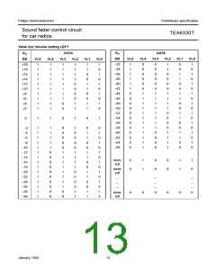
volume control of left channel (balance control)
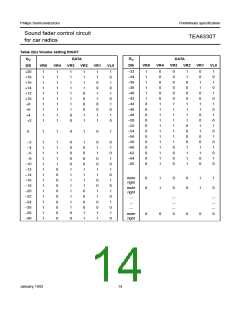
volume control of right channel (balance control)
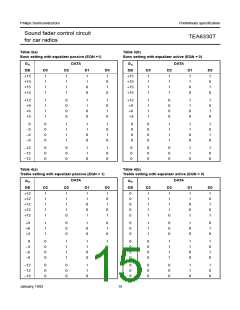
bass control of both channels
treble control of both channels
fader control front to rear
FCH
MFN
GMU
EQN
select fader channels front or rear
mute control of the selected channels front or rear
mute control, general mute
equalizer switchover (0 = equalizer-on)
January 1992
12

 NXP [ NXP ]