Philips Semiconductors
Preliminary specification
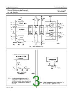
Sound fader control circuit
for car radios
TEA6330T
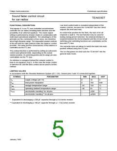
CHARACTERISTICS
V = 8.5 V; load resistors at audio outputs 10 kΩ, f = 1 kHz (R = 600 Ω), bass and treble in linear position, fader in off
P
i
S
position and T
= 25 °C; measurements taken in Fig.1 unless otherwise specified.
amb
SYMBOL
PARAMETER
CONDITIONS
MIN.
TYP.
8.5
MAX.
10
UNIT
V
supply voltage range (pin 18)
supply current
7
V
P
I
−
26
−
mA
V
P
V
V
reference voltage (pin 20)
DC voltage at output (pins 7, 8, 13, 14)
0.45 V
0.5 V
0.5 V
0.55 V
P
ref
O
P
P
P
−
−
V
Measurements over all
V
maximum AF input level for THD = 2 % G = −66 to −6 dB
v
i
at pins 2 and 19 (RMS value)
and V = 8.1 V
2
−
−
V
P
V
maximum AF output level for THD = 2% G = −4 to +20 dB
o
v
at pins 7, 8, 13, 14 (RMS value)
maximum gain by volume setting
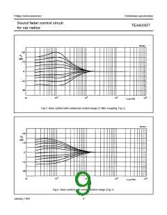
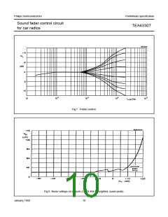
frequency response
and V = 8.1 V
1.1
19
−
−
V
P
G
B
20
21
dB
v
−1 dB roll-off frequency
35 to
−
20000
90
−
−
Hz
dB
α
crosstalk attenuation
f = 250 to 10000 Hz
CR
G = 0 dB
70
v
THD
RR
total harmonic distortion
f = 20 to 12500 Hz
V
V
V
= 50 mV
= 500 mV
= 1.6 V
G = +20 dB
−
−
−
0.1
0.3
0.2
0.5
%
%
%
i (RMS)
i (RMS)
i (RMS)
v
G = 0 dB
0.05
0.2
v
G = −10 dB
v
ripple rejection for V < 200 mV RMS
G = 0 dB
R
v
f = 100 Hz
−
−
−
70
60
50
−
−
−
dB
dB
dB
f = 40 Hz to 3 kHz
f = 3 to 12.5 kHz
mute position
P
noise power at output of a 25 W
powerstage with 26 dB gain
(only contribution of TEA6330T)
N
(V = 0)
9
−
−
−
10
nW
dB
α
crosstalk attenuation between SDA, SCL
and signal output
BUS
G = 0 dB
110
−
v
(20 log V
(p-p)/V RMS)
o
BUS
S/N(W)
weighted signal-to-noise ratio for
CCIR 468-2 quasi
peak for 6 W power
amplifier
V = 50 mV RMS
P = 50 mW
−
65
67
72
78
72
86
−
−
−
−
−
−
dB
dB
dB
dB
dB
dB
i
o
V = 500 mV RMS
P = 50 mW
−
i
o
V = 50 mV RMS
P = 1 W
65
71
−
i
o
V = 500 mV RMS
P = 1 W
o
i
V = 50 mV RMS
P = 6 W; Fig.9
o
i
V = 500 mV RMS
P = 6 W; Fig.9
−
i
o
January 1992
6

 NXP [ NXP ]