Philips Semiconductors
Preliminary specification
Sound fader control circuit
for car radios
TEA6330T
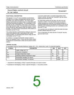
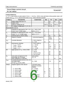
SYMBOL
PARAMETER
CONDITIONS
MIN.
TYP.
MAX.
UNIT
Audio frequency outputs QLF, QRF, QLR and QRR
V
maximum output signal (RMS value)
output resistance (pins 7, 8, 13 and 14)
admissible output load resistor
1.1
−
−
V
o
R
R
C
−
100
−
150
−
Ω
o
to ground or V
7.5
−
kΩ
nF
L
CC
admissible output load capacitor
weighted noise voltage at output
−
2.5
L
V
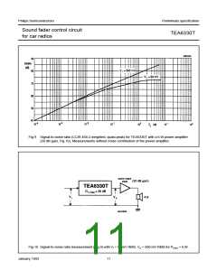
CCIR 468-2 ; Fig.8
quasi peak
N(W)
for maximum gain
for 0 dB gain
G = +20 dB
−
−
−
−
110
25
19
11
220
50
µV
µV
µV
µV
v
G = 0 dB
v
for minimum gain
for mute position
G = −66 dB
38
v
(V = 0)
22
9
R = 600Ω
Volume control
G
R
input resistance (pins 2 and 19)
volume control range
step width
35
−66
−
50
−
65
+20
-
kΩ
dB
dB
dB
dB
dB
dB
l
G
Table 2
v
∆G
2
v
gain set error
G = −50 to +20 dB
−
−
2
v
G = −66 to −50 dB
−
−
3
v
gain tracking error
balance in mid position
set mute-bits
−
−
2
α
mute attenuation at volume mute
76
90
−
mute
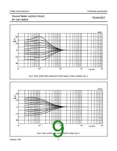
Bass control
G
controllable bass range
maximum boost
Table 3; Fig.6
f = 40 Hz
v
14
12
11
15
13
12
11
3
16
14
13
12
3.5
dB
dB
dB
dB
dB
maximum boost
f = 100 Hz
f = 40 Hz
maximum attenuation
maximum attenuation
step width
f = 100 Hz
f = 40 Hz
10
2.5
∆G
v
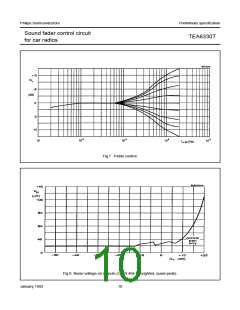
Treble control
G
controllable treble range
maximum boost
Table 4; Fig.7
f = 10 kHz
f = 15 kHz
f > 15 kHz
f = 10 kHz
f = 15 kHz
f = 15 kHz
v
9
10
12
−
11
13
15
11
13
3.5
dB
dB
dB
dB
dB
dB
maximum boost
11
−
maximum boost
maximum attenuation
maximum attenuation
step width
9
10
12
3
11
2.5
∆G
v
January 1992
7

 NXP [ NXP ]