Philips Semiconductors
Preliminary specification
Sound fader control circuit
for car radios
TEA6330T
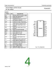
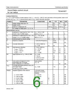
PINNING
SYMBOL
PIN
DESCRIPTION
C
1
filtering capacitor for power supply
audio input signal RIGHT
analog ground (0 V)
PS
IN-R
2
3
4
GND1
C
capacitor for bass control RIGHT
and signal to equalizer
BR1
C
C
5
6
capacitor for bass control RIGHT
BR2
capacitor for treble control RIGHT,
input signal for equalizer RIGHT
TR
QRR
QRF
7
8
right audio output signal of rear
channel
right audio output signal of front
channel
MUTE
GND2
SCL
9
input to set mute externally
10
11
12
13
digital ground (0 V) for bus control
2
clock signal of I C-bus
2
SDA
data signal of I C-bus
QLF
left audio output signal of front
channel
QLR
14
15
left audio output signal of rear
channel
C
capacitor for treble control LEFT,
input signal for equalizer LEFT
TL
C
C
16
17
capacitor for bass control LEFT
BL2
capacitor for bass control LEFT
and signal to equalizer
BL1
V
18
19
20
+8.5 V supply voltage
P
IN-L
audio input signal LEFT
Fig.4 Pin configuration.
V
reference voltage output (V /2)
P
ref
January 1992
4

 NXP [ NXP ]