Philips Semiconductors
Preliminary specification
Sound fader control circuit
TEA6320
SYMBOL
Pno(rms)
PARAMETER
CONDITIONS
MIN.
TYP. MAX. UNIT
noise output power (RMS value)
only contribution of TEA6320;
power amplifier for 6 W
mute position; note 1
−
−
10
nW
αct
note 2
−
110
−
dB
crosstalk
Vbus (p – p)
20 log-------------------------- between bus
Vo (rms)
inputs and signal outputs
Source selector
Zi
input impedance
25
−
35
45
−
kΩ
dB
dB
V
αS
input isolation of one selected
source to any other input
f = 1 kHz
105
95
f = 12.5 kHz
−
−
Vi(rms)
maximum input voltage
(RMS value)
THD < 0.5%; VCC = 8.5 V
THD < 0.5%; VCC = 7.5 V
−
2.15
1.8
−
−
−
−
V
Voffset
DC offset voltage at source
selector output by selection of any
inputs
−
10
mV
Zo
RL
CL
Gv
output impedance
−
80
−
120
Ω
output load resistance
output load capacity
10
0
−
kΩ
−
2500 pF
voltage gain, source selector
−
0
−
dB
Control part (source selector disconnected; source resistance 600 Ω)
Zi
input impedance volume input
input impedance loudness input
output impedance
100
25
−
150
33
80
−
200
40
120
−
kΩ
kΩ
Ω
Zo
RL
output load resistance
2
kΩ
nF
kΩ
CL
output load capacity
0
−
10
−
RDCL
DC load resistance at output to
ground
4.7
−
Vi(rms)
Vno
maximum input voltage
(RMS value)
THD < 0.5%
−
2.15
−
V
noise output voltage
CCIR468-2 weighted; quasi
peak
Gv = 20 dB
Gv = 0 dB
−
−
−
−
−
−
−
−
110
33
13
10
106
86
1
220
50
22
−
µV
µV
µV
µV
dB
dB
dB
dB
Gv = −66 dB
mute position
CRtot
Gstep
total continuous control range
recommended control range
step resolution
−
−
−
step error between any adjoining
step
−
0.5
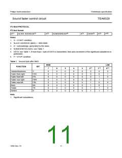
1995 Dec 19
8

 NXP [ NXP ]