Philips Semiconductors
Preliminary specification
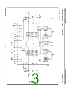
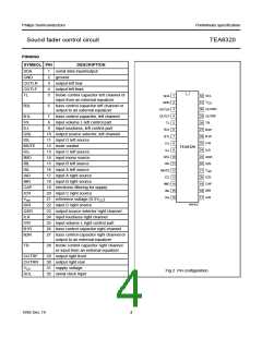
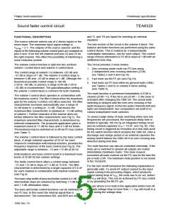
Sound fader control circuit
TEA6320
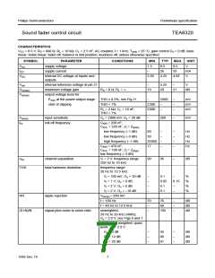
CHARACTERISTICS
VCC = 8.5 V; RS = 600 Ω; RL = 10 kΩ; CL = 2.5 nF; AC coupled; f = 1 kHz; Tamb = 25 °C; gain control Gv = 0 dB; bass
linear; treble linear; fader off; balance in mid position; loudness off; unless otherwise specified.
SYMBOL PARAMETER CONDITIONS MIN.
VCC supply voltage 7.5
TYP. MAX. UNIT
8.5
26
9.5
33
V
ICC
supply current
−
mA
V
VDC
internal DC voltage at inputs and
outputs
3.83
4.25
4.68
Vref
internal reference voltage at pin 21
maximum voltage gain
−
4.25
20
−
V
Gv(max)
Vo(rms)
RS = 0 Ω; RL = ∞
19
21
dB
output voltage level for
Pmax at the power output stage
start of clipping
THD ≤ 0.5%; see Fig.11
−
2000
−
−
−
mV
mV
mV
THD = 1%
2300
2000
−
−
RL = 2 kΩ; CL = 10 nF;
THD = 1%
Vi(rms)
fro
input sensitivity
roll-off frequency
Vo = 2000 mV; Gv = 20 dB
−
200
−
mV
CKIN = 220 nF;
CKVL = 220 nF; Zi = Zi(min)
low frequency (−1 dB)
low frequency (−3 dB)
high frequency (−1 dB)
60
−
−
−
−
−
−
−
−
Hz
Hz
Hz
Hz
30
20000
17
C
KIN = 470 nF;
CKVL = 100 nF; Zi = Zi(typ)
low frequency (−3 dB)
αcs
channel separation
Vi = 2 V; frequency range
250 Hz to 10 kHz
90
96
−
dB
THD
total harmonic distortion
frequency range
20 Hz to 12.5 kHz
Vi = 100 mV; Gv = 20 dB
Vi = 1 V; Gv = 0 dB
−
−
−
−
0.1
0.05
0.1
−
%
%
%
%
0.15
−
Vi = 2 V; Gv = 0 dB
Vi = 2 V; Gv = −10 dB
0.1
−
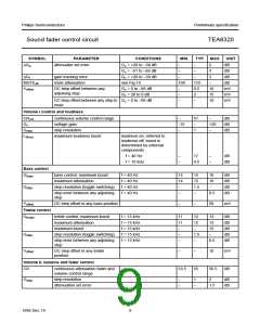
RR
ripple rejection
Vr(rms) < 200 mV
f = 100 Hz
70
−
76
−
−
−
dB
dB
dB
f = 40 Hz to 12.5 kHz
66
(S+N)/N
signal-plus-noise to noise ratio
unweighted;
−
105
20 Hz to 20 kHz (RMS);
Vo = 2.0 V; see Figs 6 and 7
CCIR468-2 weighted; quasi
peak; Vo = 2.0 V
Gv = 0 dB
Gv = 12 dB
Gv = 20 dB
−
−
−
95
88
81
−
−
−
dB
dB
dB
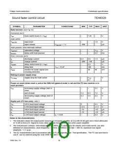
1995 Dec 19
7

 NXP [ NXP ]