Philips Semiconductors
Preliminary specification
Sound fader control circuit
TEA6320
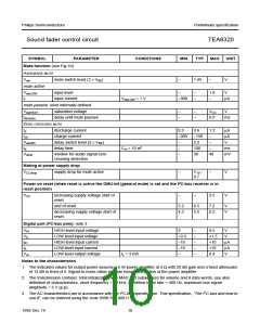
SYMBOL
PARAMETER
CONDITIONS
MIN.
TYP. MAX. UNIT
Mute function (see Fig.10)
HARDWARE MUTE
Vsw
mute switch level (2 × VBE
)
−
1.45
−
V
mute active
VswLOW
Ii
input level
−
−
−
1.0
V
input current
VswLOW = 1 V
−300
−
µA
mute passive: level internally defined
VswHIGH
td(mute)
saturation voltage
−
−
−
−
VCC
0.5
V
delay until mute passive
ms
ZERO CROSSING MUTE
Id
discharge current
charge current
0.3
−300
−
0.6
1.2
−
µA
µA
V
Ich
−150
2.2
VswDEL
td
delay switch level (3 × VBE
)
−
delay time
Cm = 10 nF
−
100
30
−
ms
mV
Vwind
window for audio signal zero
crossing detection
−
40
Muting at power supply drop
VCCdrop supply drop for mute active
−
V19
0.7
−
−
V
Power-on reset (when reset is active the GMU-bit (general mute) is set and the I2C-bus receiver is in
reset position)
VCC
increasing supply voltage start of
reset
−
−
2.5
V
end of reset
5.2
4.2
6.5
5.5
7.2
6.2
V
V
decreasing supply voltage start of
reset
Digital part (I2C-bus pins); note 3
ViH
ViL
IiH
HIGH level input voltage
3
−
−
−
−
−
9.5
V
LOW level input voltage
HIGH level input current
LOW level input current
LOW level output voltage
−0.3
−10
−10
−
+1.5
+10
+10
0.4
V
µA
µA
V
IiL
VoL
IL = 3 mA
Notes to the characteristics
1. The indicated values for output power assume a 6 W power amplifier at 4 Ω with 20 dB gain and a fixed attenuator
of 12 dB in front of it. Signal-to-noise ratios exclude noise contribution of the power amplifier.
2. The transmission contains: total initialization with MAD and subaddress for volume and 8 data words, see also
definition of characteristics, clock frequency = 50 kHz, repetition burst rate = 400 Hz, maximum bus signal
amplitude = 5 V (p-p).
3. The AC characteristics are in accordance with the I2C-bus specification. This specification, “The I2C-bus and how to
use it”, can be ordered using the code 9398 393 40011.
1995 Dec 19
10

 NXP [ NXP ]