Philips Semiconductors
Preliminary specification
Sound fader control circuit
TEA6320
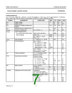
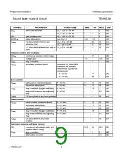
SYMBOL
∆Ga
PARAMETER
attenuator set error
CONDITIONS
Gv = +20 to −50 dB
Gv = −51 to −66 dB
Gv = +20 to −50 dB
see Fig.10
MIN.
TYP. MAX. UNIT
−
−
2
dB
dB
dB
dB
mV
mV
mV
−
−
3
∆Gt
gain tracking error
mute attenuation
−
−
2
MUTEatt
Voffset
100
−
110
0.2
2
−
DC step offset between any
adjoining step
Gv = 0 to −66 dB
Gv = 20 to 0 dB
10
15
10
−
DC step offset between any step to Gv = 0 to −66 dB
−
−
mute
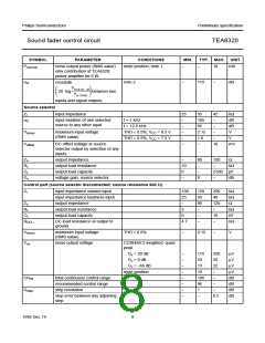
Volume I control and loudness
CRvol
Gv
continuous volume control range
−
51
−
−
dB
dB
dB
voltage gain
−31
−
+20
−
Gstep
LBmax
step resolution
1
maximum loudness boost
loudness on; referred to
loudness off; boost is
determined by external
components
f = 40 Hz
−
−
17
−
−
dB
dB
f = 10 kHz
4.5
Bass control
Gbass
bass control, maximum boost
maximum attenuation
f = 40 Hz
f = 40 Hz
f = 40 Hz
f = 40 Hz
14
14
−
15
15
1.5
−
16
16
−
dB
dB
dB
dB
Gstep
step resolution (toggle switching)
step error between any adjoining
step
−
0.5
Voffset
DC step offset in any bass position
−
−
20
mV
Treble control
Gtreble
treble control, maximum boost
maximum attenuation
f = 15 kHz
f = 15 kHz
f > 15 kHz
f = 15 kHz
f = 15 kHz
11
11
−
12
12
−
13
13
15
−
dB
dB
dB
dB
dB
maximum boost
Gstep
step resolution (toggle switching)
−
1.5
−
step error between any adjoining
step
−
0.5
Voffset
DC step offset in any treble
position
−
−
10
mV
Volume II, balance and fader control
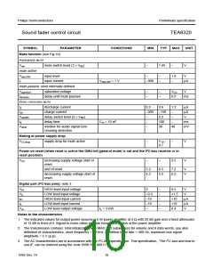
CR
continuous attenuation fader and
53.5
55
56.5
dB
volume control range
Gstep
step resolution
−
−
1
2
dB
dB
attenuation set error
−
1.5
1995 Dec 19
9

 NXP [ NXP ]