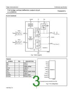
Philips Semiconductors
Preliminary specification
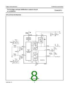
Full bridge vertical deflection output circuit
in LVDMOS
TDA8357J
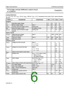
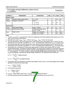
SYMBOL
PARAMETER
CONDITIONS
MIN.
TYP. MAX. UNIT
Flyback switch
Io(peak)
maximum (peak) output current
voltage loss at flyback
t ≤ 1.5 ms
note 11
Io = 0.7 A
−
−
±1.2
A
Vloss(FB)
−
−
7.5
8
8.5
9
V
V
Io = 1.0 A
Guard circuit
VO(grd)
guard output voltage
IO(grd) = 100 µA
5
6
7
V
V
VO(grd)(max) allowable guard voltage
maximum leakage current
−
−
18
IL(max) = 10 µA
IO(grd)
output current
VO(grd) = 0 V; not active
VO(grd) = 4.5 V; active
−
−
−
10
µA
1
2.5
mA
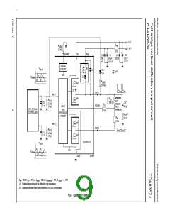
Notes
1. To limit VOUTA to 68 V, VFB must be 66 V due to the voltage drop of the internal flyback diode between pins OUTA
and VFB at the first part of the flyback.
2. Allowable input range: VI(bias) + Vi(dif) < 1600 mV and VI(bias) − Vi(dif) > 100 mV for each input.
3. This value specifies the sum of the voltage losses of the internal current paths between pins VP and OUTA, and
between pins OUTB and GND. Specified for Tj = 125 °C. The temperature coefficient for Vloss(1) is a positive value.
4. This value specifies the sum of the voltage losses of the internal current paths between pins VP and OUTB, and
between pins OUTA and GND. Specified for Tj = 125 °C. The temperature coefficient for Vloss(2) is a positive value.
5. The linearity error is measured for a linear input signal without S-correction and is based on the ‘on screen’
measurement principle. This method is defined as follows. The output signal is divided in 22 successive equal time
blocks k. The 1st and 22nd blocks are ignored, while the voltage amplitudes are measured across RM, starting at
k = 2 and ending at k = 21, where Vk and Vk+1 are the measured voltages of two successive blocks. Vmin, Vmax and
Vavg are the minimum, maximum and average voltages respectively. The linearity errors are defined as:
Vk – Vk + 1
a) LE =
b) LE =
(adjacent blocks)
-------------------------
Vavg
V
max – Vmin
(non adjacent blocks)
-------------------------------
Vavg
6. The linearity errors are specified for a minimum input voltage of 300 mV (p-p). Lower input voltages lead to voltage
dependent S-distortion in the input stage.
V
OUTA – VOUTB
-------------------------------------------
FEEDB – VOUTB
7. G v(ol)
=
V
8. Pin FEEDB not connected.
V
FEEDB – V
-------------------------------O----U----T---B-
INA – VINB
9. G v
=
V
10. VP(ripple) = 500 mV (RMS value); 50 Hz < fP(ripple) < 1 kHz; measured across RM.
11. This value specifies the internal voltage loss of the current path between pins VFB and OUTA.
1999 Nov 10
7

 NXP [ NXP ]