Philips Semiconductors
Preliminary specification
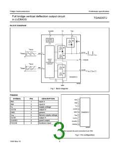
Full bridge vertical deflection output circuit
in LVDMOS
TDA8357J
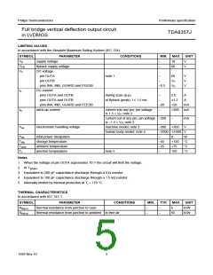
CHARACTERISTICS
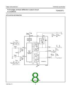
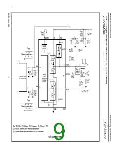
VP = 12 V; VFB = 45 V; fvert = 50 Hz; VI(bias) = 880 mV; Tamb = 25 °C; measured in test circuit of Fig.3; unless otherwise
specified.
SYMBOL
Supplies
PARAMETER
CONDITIONS
MIN.
TYP. MAX. UNIT
VP
operating supply voltage
flyback supply voltage
7.5
12
45
10
55
−
18
66
15
75
10
V
VFB
note 1
2VP
−
V
Iq(P)(av)
Iq(P)
average quiescent supply current
quiescent supply current
during scan
mA
mA
mA
no signal; no load
during scan
−
Iq(FB)(av)
average quiescent flyback supply
current
−
Inputs A and B
Vi(dif)(p-p)
differential input voltage
note 2
note 2
−
1000 1500 mV
(peak-to-peak value)
input bias voltage
input bias current
VI(bias)
II(bias)
100
880
25
1600 mV
−
35
µA
Outputs A and B
Vloss(1) voltage loss first scan part
note 3
Io = 0.7 A
Io = 1.0 A
note 4
−
−
−
−
3.9
5.5
V
V
Vloss(2)
voltage loss second scan part
Io = −0.7 A
Io = −1.0 A
−
−
−
−
−
−
2.8
4.0
2.0
V
V
A
Io(p-p)
LE
output current (peak-to-peak value)
linearity error
Io(p-p) = 2.0 A; notes 5 and 6
adjacent blocks
−
−
1
1
2
3
%
%
non adjacent blocks
Voffset
offset voltage
across RM; Vi(dif) = 0 V
V
I(bias) = 200 mV
I(bias) = 1 V
−
−
−
−
−
−
−
−
−
±15
±25
40
−
mV
mV
µV/K
V
V
−
∆Voffset(T)
VO
offset voltage variation with temperature across RM; Vi(dif) = 0 V
−
DC output voltage
Vi(dif) = 0 V
notes 7 and 8
open-loop
note 9
0.5VP
Gv(ol)
f−3dB(h)
Gv
open-loop voltage gain
high −3 dB cut-off frequency
voltage gain
60
1
−
dB
−
kHz
1
−
10−4
∆Gv(T)
voltage gain variation with the
temperature
−
K−1
dB
PSRR
power supply rejection ratio
note 10
80
90
−
1999 Nov 10
6

 NXP [ NXP ]