Philips Semiconductors
Preliminary specification
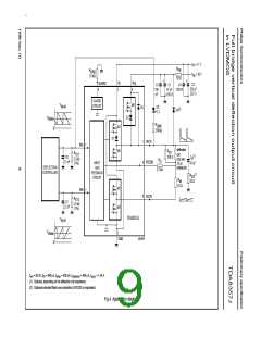
Full bridge vertical deflection output circuit
in LVDMOS
TDA8357J
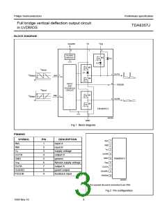
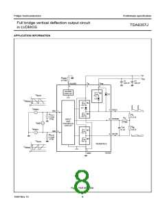
BLOCK DIAGRAM
V
V
GUARD
8
P
FB
6
handbook, full pagewidth
3
GUARD
CIRCUIT
M5
D2
D3
M2
M4
V
i(p-p)
D1
OUTA
7
V
1
INA
I(bias)
0
9
4
INPUT
AND
FEEDBACK
CIRCUIT
FEEDB
V
i(p-p)
M1
M3
INB
V
2
I(bias)
0
OUTB
TDA8357J
5
MGS803
GND
Fig.1 Block diagram.
PINNING
handbook, halfpage
SYMBOL
INA
PIN
DESCRIPTION
input A
INA
1
2
3
4
5
6
7
8
9
1
2
3
4
5
6
7
8
9
INB
INB
input B
V
P
VP
supply voltage
output B
OUTB
GND
OUTB
GND
VFB
TDA8357J
ground
V
flyback supply voltage
output A
FB
OUTA
GUARD
FEEDB
OUTA
GUARD
FEEDB
guard output
feedback input
MGS804
The exposed die pad is connected to pin GND.
Fig.2 Pin configuration.
1999 Nov 10
3

 NXP [ NXP ]