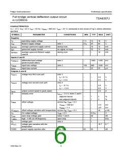
Philips Semiconductors
Preliminary specification
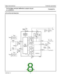
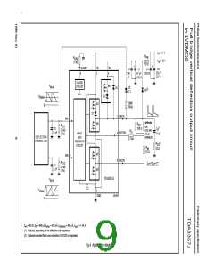
Full bridge vertical deflection output circuit
in LVDMOS
TDA8357J
Supply voltage calculation
The flyback supply voltage calculated this way is about
5% to 10% higher than required.
For calculating the minimum required supply voltage,
several specific application parameter values have to be
known. These parameters are the required
maximum (peak) deflection coil current Icoil(peak), the coil
parameters Rcoil and Lcoil, and the measuring resistance
of RM. The required maximum (peak) deflection coil
current should also include the overscan.
Calculation of the power dissipation of the vertical
output stage
The IC total power dissipation is given by the formula:
Ptot = Psup − PL
The power to be supplied is given by the formula:
The deflection coil resistance has to be multiplied with 1.2
in order to take account of hot conditions.
I
Psup = V × coil(peak) + V × 0.015 [A] + 0.3 [W]
-----------------------
P
P
2
Chapter “Characteristics” supplies values for the voltage
losses of the vertical output stage. For the first part of the
scan the voltage loss is given by Vloss(1). For the second
In this formula 0.3 [W] represents the average value of the
losses in the flyback supply.
part of the scan the voltage loss is given by Vloss(2)
.
The average external load power dissipation in the
deflection coil and the measuring resistor is given by the
formula:
The voltage drop across the deflection coil during scan is
determined by the coil impedance. For the first part of the
scan the inductive contribution and the ohmic contribution
to the total coil voltage drop are of opposite sign, while for
the second part of the scan the inductive part and the
ohmic part have the same sign.
2
(Icoil(peak)
)
PL
=
× (R coil + RM)
-------------------------------
3
For the vertical frequency the maximum frequency
occurring must be applied to the calculations.
Example
Table 1 Application values
SYMBOL VALUE
Icoil(peak)
The required power supply voltage VP for the first part of
the scan is given by:
UNIT
0.725
1.45
8.82
7.9
A
VP(1) = Icoil(peak) × (Rcoil + RM)
– Lcoil × 2Icoil(peak) × fvert(max) + Vloss(1)
Icoil(p-p)
Lcoil
Rcoil
RM
A
mH
Ω
The required power supply voltage VP for the second part
of the scan is given by:
1.5
Ω
VP(2) = Icoil(peak) × (Rcoil + RM)
+ Lcoil × 2Icoil(peak) × fvert(max) + Vloss(2)
fvert
50
Hz
µs
tFB
640
The minimum required supply voltage VP shall be the
highest of the two values VP(1) and VP(2). Spread in supply
voltage and component values also has to be taken into
account.
Table 2 Calculated values
SYMBOL VALUE
UNIT
VP
11
V
Ω
s
RM + Rcoil (hot)
11
Flyback supply voltage calculation
tvert
x
0.02
0.000802
29
If the flyback time is known, the required flyback supply
voltage can be calculated by the simplified formula:
VFB
Psup
PL
V
R
1 – e–t
coil + RM
4.45
1.93
2.52
W
W
W
VFB = Icoil(p–p)
×
--------------------------
FB ⁄ x
Ptot
where:
L coil
x =
--------------------------
R
coil + RM
1999 Nov 10
10

 NXP [ NXP ]