Philips Semiconductors
Preliminary specification
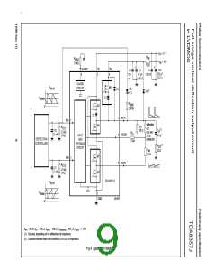
Full bridge vertical deflection output circuit
in LVDMOS
TDA8357J
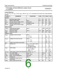
LIMITING VALUES
In accordance with the Absolute Maximum Rating System (IEC 134).
SYMBOL
PARAMETER
CONDITIONS
MIN. MAX. UNIT
VP
supply voltage
−
−
18
68
V
V
VFB
Vn
flyback supply voltage
DC voltage
pin OUTA
note 1
−
68
VP
VP
V
V
V
pin OUTB
−
pins INA, INB, GUARD and FEEDB
DC current
−0.5
In
pins OUTA and OUTB
pins OUTA and OUTB
pins INA, INB, GUARD and FEEDB
latch-up current
during scan (p-p)
−
2.0
A
at flyback (peak); t ≤ 1.5 ms
−
±1.2
+20
A
−20
−
mA
Ilu
current into any pin; pin voltage
+200 mA
is 1.5 × VP; note 2
current out of any pin; pin voltage −200
is −1.5 × VP; note 2
−
mA
Ves
electrostatic handling voltage
machine model; note 3
−300
+300
V
human body model; note 4
−2000 +2000 V
Ptot
Tstg
Tamb
Tj
total power dissipation
storage temperature
ambient temperature
junction temperature
−
8
W
−55
−25
−
+150 °C
+75
150
°C
°C
note 5
Notes
1. When the voltage at pin OUTA supersedes 70 V the circuit will limit the voltage.
2. At Tj(max)
.
3. Equivalent to 200 pF capacitance discharge through a 0 Ω resistor.
4. Equivalent to 100 pF capacitance discharge through a 1.5 kΩ resistor.
5. Internally limited by thermal protection at Tj ≈ 170 °C.
THERMAL CHARACTERISTICS
In accordance with IEC 747-1.
SYMBOL
Rth(j-c)
PARAMETER
CONDITIONS
MIN.
TYP. MAX. UNIT
thermal resistance from junction to case
−
−
−
6
K/W
K/W
Rth(j-a)
thermal resistance from junction to ambient in free air
−
65
1999 Nov 10
5

 NXP [ NXP ]