Philips Semiconductors
Preliminary specification
Full bridge vertical deflection output circuit
in LVDMOS
TDA8357J
FEATURES
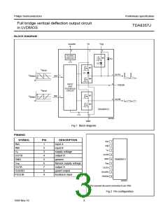
GENERAL DESCRIPTION
• Few external components required
The TDA8357J is a power circuit for use in 90° and 110°
colour deflection systems for 25 to 200 Hz field
• High efficiency fully DC coupled vertical bridge output
frequencies, and for 4 : 3 and 16 : 9 picture tubes. The IC
contains a vertical deflection output circuit, operating as a
high efficiency class G system. The full bridge output
circuit allows DC coupling of the deflection coil in
combination with single positive supply voltages.
circuit
• Vertical flyback switch with short rise and fall times
• Built-in guard circuit
• Thermal protection circuit
• Improved EMC performance due to differential inputs.
The IC is constructed in a Low Voltage DMOS (LVDMOS)
process that combines bipolar, CMOS and DMOS
devices. DMOS transistors are used in the output stage
because of absence of second breakdown.
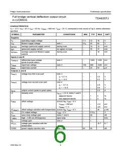
QUICK REFERENCE DATA
SYMBOL
Supplies
PARAMETER
CONDITIONS
MIN.
TYP. MAX. UNIT
VP
supply voltage
7.5
12
45
10
−
18
66
15
10
8
V
VFB
flyback supply voltage
2VP
−
V
Iq(P)(av)
Iq(FB)(av)
Ptot
average quiescent supply current
average quiescent flyback supply current
total power dissipation
during scan
during scan
mA
mA
W
−
−
−
Inputs and outputs
Vi(dif)(p-p) differential input voltage (peak-to-peak value)
Io(p-p)
−
−
1000 1500 mV
output current (peak-to-peak value)
−
2.0
A
Flyback switch
Io(peak)
maximum (peak) output current
t ≤ 1.5 ms
−
−
±1.2
A
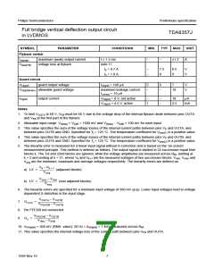
Thermal data; in accordance with IEC 747-1
Tstg
Tamb
Tj
storage temperature
ambient temperature
junction temperature
−55
−25
−
−
−
−
+150 °C
+75
150
°C
°C
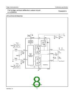
ORDERING INFORMATION
TYPE
PACKAGE
DESCRIPTION
NUMBER
NAME
VERSION
TDA8357J
DBS9P
plastic DIL-bent-SIL power package; 9 leads (lead length
12/11 mm); exposed die pad
SOT523-1
1999 Nov 10
2

 NXP [ NXP ]