Philips Semiconductors
Product specification
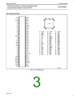
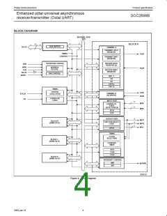
Enhanced octal universal asynchronous
receiver/transmitter (Octal UART)
SCC2698B
DESCRIPTION
FEATURES
The SCC2698B Enhanced Octal Universal Asynchronous
Receiver/Transmitter (Octal UART) is a single chip MOS-LSI
communications device that provides eight full-duplex asynchronous
receiver/transmitter channels in a single package. It is fabricated
with CMOS technology which combines the benefits of high density
and low power consumption.
• Eight full-duplex independent asynchronous receiver/transmitters
• Quadruple buffered receiver data register
• Programmable data format:
– 5 to 8 data bits plus parity
– Odd, even, no parity or force parity
– 1, 1.5 or 2 stop bits programmable in 1/16-bit increments
The operating speed of each receiver and transmitter can be
selected independently as one of 26 fixed baud rates, a 16X clock
derived from a programmable counter/timer, or an external 1X or
16X clock. The baud rate generator and counter/timer can operate
directly from a crystal or from external clock inputs. The ability to
independently program the operating speed of the receiver and
transmitter make the Octal UART particularly attractive for
dual-speed channel applications such as clustered terminal
systems.
• Baud rate for the receiver and transmitter selectable from:
– 26 fixed rates: 50 to 38.4K baud
Non-standard rates to 115.2K baud
– User-defined rates from the programmable counter/timer
associated with each of four blocks
– External 1x or 16x clock
• Parity, framing, and overrun error detection
• False start bit detection
• Line break detection and generation
• Programmable channel mode
The receiver is quadruple buffered to minimize the potential of
receiver overrun or to reduce interrupt overhead in interrupt driven
systems. In addition, a handshaking (RTS/CTS) capability is
provided to disable a remote UART transmitter when the receiver
buffer is full.
– Normal (full-duplex), automatic echo, local loop back, remote
loopback
• Four multi-function programmable 16-bit counter/timers
• Four interrupt outputs with eight maskable interrupting conditions
The UART provides a power-down mode in which the oscillator is
frozen but the register contents are stored. This results in reduced
power consumption on the order of several magnitudes. The Octal
UART is fully TTL compatible and operates from a single +5V power
supply.
for each output
• Receiver ready/FIFO full and transmitter ready status available on
16 multi-function pins in PLCC package
• On-chip crystal oscillator
• TTL compatible
• Single +5V power supply with low power mode
• Eight multi-purpose output pins
• Sixteen multi-purpose I/O pins
The SCC2698B is an upwardly compatible version of the 2698A
Octal UART. In PLCC packaging, it is enhanced by the addition of
receiver ready or FIFO full status outputs, and transmitter empty
status outputs for each channel on 16 multipurpose I/O pins. The
multipurpose pins of the 2698B RIO pins, thus DMA and modem
control is provided.
• Sixteen multi-purpose Input pins with pull-up resistors
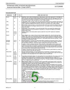
ORDERING INFORMATION
COMMERCIAL
INDUSTRIAL
DWG #
PACKAGES
V
CC
= +5V +5%, T = 0°C to +70°C
V
CC
= +5V +5%, T = –40°C to +85°C
A
A
84-PinPlasticLeadedChipCarrier(PLCC)
SCC2698BC1A84
SCC2698BE1A84
SOT189-3
NOTE: Pin Grid Array (PGA) package version is available from Philips Components Military Division.
1
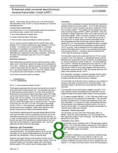
ABSOLUTE MAXIMUM RATINGS
SYMBOL
PARAMETER
RATING
Note 4
UNIT
2
o
T
Operating ambient temperature range
C
A
o
T
Storage temperature range
–65 to +150
–0.5 to +7.0
C
STG
3
V
V
P
Voltage from V to GND
V
V
CC
DD
3
Voltage from any pin to ground
Power dissipation
–0.5 to V +0.5
S
CC
1
W
D
NOTES:
1. Stresses above those listed under Absolute Maximum Ratings may cause permanent damage to the device. This is a stress rating only and
functional operation of the device at these or any other condition above those indicated in the operation section of this specification is not
implied.
2. For operating at elevated temperatures, the device must be derated based on +150°C maximum junction temperature.
3. This product includes circuitry specifically designed for the protection of its internal devices from damaging effects of excessive static
charge. Nonetheless, it is suggested that conventional precautions be taken to avoid applying any voltages larger than the rated maxima.
4. Parameters are valid over specified temperature range. See ordering information table for applicable temperature range and operating
supply range.
2
2000 Jan 31
853-1127 23062

 NXP [ NXP ]