Philips Semiconductors
Product specification
Enhanced octal universal asynchronous
receiver/transmitter (Octal UART)
SCC2698B
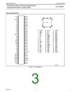
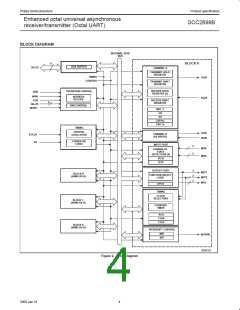
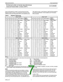
PIN DESCRIPTION
PIN
NO.
MNEMONIC
D0–D7
TYPE
NAME AND FUNCTION
8–13,
16, 17
I/O
Data Bus: Active–High 8-bit bidirectional 3-State data bus. Bit 0 is the LSB and bit 7 is the MSB. All
data, command, and status transfers between the CPU and the Octal UART take place over this bus.
The direction of the transfer is controlled by the WRN and RDN inputs when the CEN input is low.
When the CEN input is High, the data bus is in the 3-State condition.
CEN
18
19
22
I
I
I
I
I
Chip Enable: Active-Low input. When Low, data transfers between the CPU and the Octal UART are
enabled on D0–D7 as controlled by the WRN, RDN and A0–A5 inputs. When CEN is High, the Octal
UART is effectively isolated from the data bus and D0–D7 are placed in the 3-State condition.
WRN
RDN
Write Strobe: Active-Low input. A Low on this pin while CEN is Low causes the contents of the data
bus to be transferred to the register selected by A0–A5. The transfer occurs on the trailing (rising)
edge of the signal.
Read Strobe: Active-Low input. A Low on this pin while CEN is Low causes the contents of the
register selected by A0–A5 to be placed on the data bus. The read cycle begins on the leading
(falling) edge of RDN.
A0–A5
RESET
23, 25,
27, 29,
31, 32
Address Inputs: Active-High address inputs to select the Octal UART registers for read/write
operations.
15
Reset: Master reset. A High on this pin clears the status register (SR), clears the interrupt mask
register (IMR), clears the interrupt status register (ISR), clears the output port configuration register
(OPCR), places the receiver and transmitter in the inactive state causing the TxD output to go to the
marking (High) state, and stops the counter/timer. Clears power-down mode and interrupts. Clears
Test Modes, sets MR pointer to MR1.
INTRAN–
INTRDN
35, 36,
46, 47
O
I
Interrupt Request: This active-Low open drain output is asserted on occurrence of one or more of
eight maskable interrupting conditions. The CPU can read the interrupt status register to determine
the interrupting condition(s). These pins require a pullup device and may be wire ORed.
X1/CLK
7
Crystal 1: Crystal or external clock input. When using the crystal oscillator, this pin serves as the
connection for one side of the crystal. If a crystal is not used, an external clock is supplied at this
input. An external clock (or crystal) is required even if the internal baud rate generator is not utilized.
This clock is used to drive the internal baud rate generator, as an optional input to the timer/counter,
and to provide other clocking signals required by the chip.
X2
6
I
I
Crystal 2: Connection for other side of crystal. If an external source is used instead of a crystal, this
connection should be left open (see Figure 9).
RxDa–RxDh
3, 56,
Receiver Serial Data Input: The least significant bit is received first. If external receiver clock is
specified, this input is sampled on the rising edge of the clock. If internal clock is used, the RxD input
is sampled on the rising edge of the RxC1x signal as seen on the MPO pin.
83, 57,
79, 58,
75, 59
TxDa–TxDh
1, 41,
O
O
Transmitter Serial Data Output: The least significant bit is transmitted first. This output is held in the
marking (High) condition when the transmitter is idle or disabled and when the Octal UART is
operating in local loopback mode. If external transmitter is specified, the data is shifted on the falling
edge of the transmitter clock. If internal clock is used, the TxD output changes on the falling edge of
the TxC1x signal as seen on the MPO pin.
81, 49,
74, 52,
73, 55
MPOa–MPOh
72, 43,
71, 51,
69, 53,
67, 54
Multi-Purpose Output: Each of the four DUARTS has two MPO pins (one per UART). One of the
following eight functions can be selected for this output pin by programming the OPCR (output port
configuration register). Note that reset conditions MPO pins to RTSN.
RTSN – Request to send active-Low output. This output is asserted and negated via the command
register. By appropriate programming of the mode registers, (MR1[7])=1 RTSN can be programmed to
be automatically reset after the character in the transmitter is completely shifted or when the receiver
FIFO and shift register are full. RTSN is an internal signal which normally represents the condition of
the receiver FIFO not full, i.e., the receiver can request more data to be sent. However, it can also be
controlled by the transmitter empty and the commands 8h and 9h written to the CR (command
register).
C/TO – The counter/timer output.
TxC1X – The 1X clock for the transmitter.
TxC16X – The 16X clock for the transmitter.
RxC1X – The 1X clock for the receiver.
RxC16X – The 16X clock for the receiver.
TxRDY – Transmitter holding register empty signal.
RxRDY/FFULL – Receiver FIFO not empty/full signal.
MPI0a–MPI0h
33, 34,
37, 39,
61, 63,
76, 77
I
Multi-Purpose Input 0: This pin (one in each UART) is programmable. Its state can always be read
through the IPCR bit 0, or the IPR bit 0.
CTSN: By programming MR2[4] to a 1, this input controls the clear-to-send function for the
transmitter. It is active low. This pin is provided with a change-of-state detector.
5
2000 Jan 31

 NXP [ NXP ]