Philips Semiconductors
Product specification
Dual asynchronous receiver/transmitter (DUART)
SCC2692
1, 2, 4
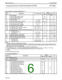
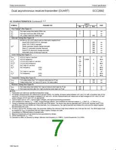
AC CHARACTERISTICS (Continued)
LIMITS
SYMBOL
Port Timing (See Figure 5)
PARAMETER
UNIT
Max
3
Min
Typ
5
Port input setup time before RDN Low
Port input hold time after RDN High
OP output valid from WRN High
0
0
ns
ns
ns
t
t
t
PS
PH
PD
400
n
Interrupt Timing (See Figure 6)
INTRN (or OP3-OP7 when used as interrupts) negated from:
Read RHR (RxRDY/FFULL interrupt)
Write THR (TxRDY interrupt)
Reset command (break change interrupt)
Stop C/T command (counter interrupt)
Read IPCR (input port change interrupt)
Write IMR (clear of interrupt mask bit)
300
300
300
300
300
300
ns
ns
ns
ns
ns
ns
9
t
IR
Clock Timing (See Figure 7)
t
100
ns
X1/CLK High or Low time
CLK
CLK
10
f
t
f
t
f
X1/CLK frequency
0
100
0
220
0
0
220
0
3.6864
4
4
MHz
ns
MHz
ns
MHz
MHz
ns
MHz
MHz
CTCLK (IP2) High or Low time
CTCLK (IP2) frequency
RxC High or Low time
CTC
CTC
RX
8
8
RxC frequency
(16X)
(1X)
2
1
RX
t
f
TxC High or Low time
TxC frequency
TX
8
(16X)
(1X)
1
1
TX
0
Transmitter Timing (See Figure 8)
t
t
TxD output delay from TxC external clock input on IP pin
Output delay from TxC low at OP pin to TxD data output
350
150
ns
ns
TXD
0
TCS
Receiver Timing (See Figure 9)
t
t
RxD data setup time before RxC high at external clock input on IP pin
RxD data hold time after RxC high at external clock input on IP pin
240
200
ns
ns
RXS
RXH
NOTES:
1. Parameters are valid over specified temperature range.
2. All voltage measurements are referenced to ground (GND). For testing, all inputs swing between 0.4V and 2.4V with a transition time of 5ns
maximum. For X1/CLK this swing is between 0.4V and 4.4V. All time measurements are referenced at input voltages of 0.8V and 2.0V and
output voltages of 0.8V and 2.0V, as appropriate.
3. Typical values are at +25°C, typical supply voltages, and typical processing parameters.
4. Test conditions for outputs: C = 150pF, except interrupt outputs. Test conditions for interrupt outputs: C = 50pF, R = 2.7KΩ to V .
L
L
L
CC
5. Timing is illustrated and referenced to the WRN and RDN inputs. The device may also be operated with CEN as the ‘strobing’ input. CEN
and RDN (also CEN and WRN) are ORed internally. As a consequence, the signal asserted last initiates the cycle and the signal negated
first terminates the cycle.
6. If CEN is used as the ‘strobing’ input, the parameter defines the minimum High times between one CEN and the next. The RDN signal must
be negated for t
to guarantee that any status register changes are valid.
RWD
7. Guaranteed by characterization of sample units.
8. Minimum frequencies are not tested but are guaranteed by design.
9. 325ns maximum for T > 70°C.
A
10.Operation to 0MHz is assured by design. Minimum test frequency is 2.0MHz. Crystal frequencies 2 to 4 MHz.
7
1998 Sep 04

 NXP [ NXP ]