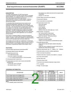
Philips Semiconductors
Product specification
Dual asynchronous receiver/transmitter (DUART)
SCC2692
INDEX
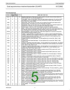
CORNER
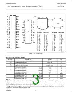
A0
IP3
A1
1
2
3
4
5
40
V
CC
6
40
1
39 IP4
38 IP5
37 IP6
36 IP2
44
34
7
39
1
33
A0
A1
1
2
3
4
5
28 V
CC
IP1
A2
27 IP2
PLCC
PQFP
CEN
A2
26
A3
IP0
6
7
8
9
35 CEN
34 RESET
33 X2
A3
25 RESET
24 X2
11
23
22
29
17
WRN
12
WRN
RDN
18
28
TOP VIEW
RDN
RxDB
TxDB
OP1
6
7
8
9
23 X1/CLK
22 RxDA
21 TxDA
20 OP0
19 D0
32 X1/CLK
31 RxDA
30 TxDA
29 OP0
TOP VIEW
RxDB 10
TxDB 11
OP1 12
DIP
DIP
PIN/FUNCTION
PIN/FUNCTION
PIN/FUNCTION
PIN/FUNCTION
1
2
NC
A0
IP3
A1
IP1
A2
A3
IP0
WRN
23 NC
24 INTRN
25 D6
26 D4
27 D2
1
2
A3
IP0
23 N/C
24 OP6
25 OP4
26 OP2
27 OP0
28 TxDA
29 RxDA
30 X1/CLK
31 X2
3
4
5
6
7
8
9
3
4
5
6
7
8
9
WRN
RDN
RxDB
TxDB
OP1
OP3
OP5
D1 10
D3 11
D5 12
OP3 13
OP5 14
OP7 15
D1 16
28 OP2
27 OP4
26 OP6
25 D0
18 D2
28 D0
29 OP6
30 OP4
31 OP2
32 OP0
33 TXDA
34 NC
17 D4
D7 13
GND 14
16 D6
10 RDN
11 RXDB
12 NC
10 OP7
11 N/C
12 D1
32 RESET
33 CEN
34 IP2
15 INTRN
D3 17
24 D2
13 TXDB
14 OP1
15 OP3
16 OP5
17 OP7
18 D1
19 D3
20 D5
21 D7
22 GND
35 RXDA
36 X1/CLK
37 X2
38 RESET
39 CEN
40 IP2
41 IP6
42 IP5
43 IP4
13 D3
14 D5
15 D7
16 GND
17 GND
18 INTRN
19 D6
20 D4
21 D2
35 IP6
36 IP5
37 IP4
D5 18
23 D4
38
39
V
V
D7 19
22 D6
CC
CC
40 A0
41 IP3
42 A1
43 IP1
44 A2
GND 20
21 INTRN
44 V
22 D0
CC
SD00131
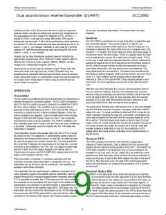
Figure 1. Pin Configurations
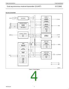
1
ABSOLUTE MAXIMUM RATINGS
SYMBOL
PARAMETER
RATING
Note 4
UNIT
°C
2
T
A
Operating ambient temperature range
T
Storage temperature range
-65 to +150
-0.5 to +7.0
°C
STG
3
V
Voltage from V to GND
V
CC
CC
3
V
Voltage from any pin to GND
Package power dissipation
Package power dissipation
Package power dissipation
Package power dissipation
Derating factor above 25°C
Derating factor above 25°C
Derating factor above 25°C
Derating factor above 25°C
-0.5 to V +0.5
V
S
CC
DIP28
DIP40
1.22
2.97
2.66
2.08
19
W
W
P
D
PLCC44
PQFP44
DIP28
W
W
mW/°C
mW/°C
mW/°C
mW/°C
DIP40
24
PLCC44
PQFP44
21
17
NOTES:
1. Stresses above those listed under Absolute Maximum Ratings may cause permanent damage to the device. This is a stress rating only and
functional operation of the device at these or any other condition above those indicated in the operation section of this specification is not
implied.
2. For operating at elevated temperatures, the device must be derated.
3. This product includes circuitry specifically designed for the protection of its internal devices from damaging effects of excessive static
charge. Nonetheless, it is suggested that conventional precautions be taken to avoid applying any voltages larger than the rated maxima.
4. Parameters are valid over specified temperature range.
3
1998 Sep 04

 NXP [ NXP ]