Philips Semiconductors
Product specification
Dual asynchronous receiver/transmitter (DUART)
SCC2692
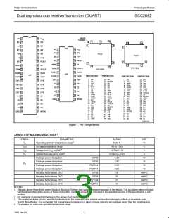
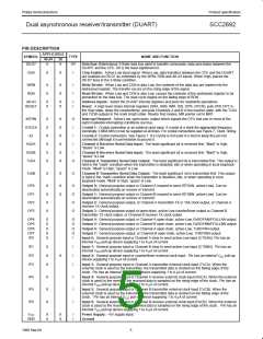
PIN DESCRIPTION
APPLICABLE
SYMBOL
TYPE
NAME AND FUNCTION
40,44
28
D0-D7
X
X
I/O
Data Bus: Bidirectional 3-State data bus used to transfer commands, data and status between the
DUART and the CPU. D0 is the least significant bit.
CEN
X
X
I
Chip Enable: Active-Low input signal. When Low, data transfers between the CPU and the DUART
are enabled on D0-D7 as controlled by the WRN, RDN and A0-A3 inputs. When High, places the
D0-D7 lines in the 3-State condition.
WRN
RDN
X
X
X
X
I
I
Write Strobe: When Low and CEN is also Low, the contents of the data bus are loaded into the
addressed register. The transfer occurs on the rising edge of the signal.
Read Strobe: When Low and CEN is also Low, causes the contents of the addressed register to be
presented on the data bus. The read cycle begins on the falling edge of RDN.
A0-A3
X
X
X
X
I
I
Address Inputs: Select the DUART internal registers and ports for read/write operations.
RESET
Reset: A High level clears internal registers (SRA, SRB, IMR, ISR, OPR, OPCR), puts OP0-OP7 in
the High state, stops the counter/timer, and puts Channels A and B in the inactive state, with the TxDA
and TxDB outputs in the mark (High) state. Resets Test modes, MR pointer set to MR1.
INTRN
X1/CLK
X2
X
X
X
X
X
X
X
X
X
X
X
X
O
I
Interrupt Request: Active-Low, open-drain, output which signals the CPU that one or more of the
eight maskable interrupting conditions are true.
Crystal 1: Crystal connection or an external clock input. A crystal of a clock the appropriate frequency
(nominally 3.6864 MHz) must be supplied at all times. For crystal connections see Figure 7, Clock Timing.
Crystal 2: Crystal connection. See Figure 7. If a crystal is not used it is best to keep this pin not
connected although it is permissible to ground it.
Channel A Receiver Serial Data Input: The least significant bit is received first. “Mark” is High,
“space” is Low.
Channel B Receiver Serial Data Input: The least significant bit is received first. “Mark” is High,
“space” is Low.
Channel A Transmitter Serial Data Output: The least significant bit is transmitted first. This output is
held in the “mark” condition when the transmitter is disabled, idle or when operating in local loopback
mode. “Mark” is High, “space” is Low.
I
RxDA
RxDB
TxDA
I
I
O
TxDB
X
X
O
Channel B Transmitter Serial Data Output: The least significant bit is transmitted first. This output
is held in the ‘mark’ condition when the transmitter is disabled, idle, or when operating in local
loopback mode. ‘Mark’ is High, ‘space’ is Low.
OP0
OP1
OP2
OP3
X
X
X
X
X
X
O
O
O
O
Output 0: General purpose output or Channel A request to send (RTSAN, active-Low). Can be
deactivated automatically on receive or transmit.
Output 1: General purpose output or Channel B request to send (RTSBN, active-Low). Can be
deactivated automatically on receive or transmit.
Output 2: General purpose output, or Channel A transmitter 1X or 16X clock output, or Channel A
receiver 1X clock output.
Output 3: General purpose output or open-drain, active-Low counter/timer output or Channel B
transmitter 1X clock output, or Channel B receiver 1X clock output.
OP4
OP5
OP6
OP7
IP0
X
X
X
X
X
O
O
O
O
I
Output 4: General purpose output or Channel A open-drain, active-Low, RxRDYAN/FFULLAN output.
Output 5: General purpose output or Channel B open-drain, active-Low, RxRDYBN/FFULLBN output.
Output 6: General purpose output or Channel A open-drain, active-Low, TxRDYAN output.
Output 7: General purpose output, or Channel B open-drain, active-Low, TxRDYBN output.
Input 0: General purpose input or Channel A clear to send active-Low input (CTSAN). Pin has an
internal V pull-up device supplying 1 to 4 mA of current.
CC
IP1
IP2
IP3
X
X
X
I
I
I
Input 1: General purpose input or Channel B clear to send active-Low input (CTSBN). Pin has an
internal V pull-up device supplying 1 to 4 mA of current.
CC
X
Input 2: General purpose input or counter/timer external clock input. Pin has an internal V pull-up
CC
device supplying 1 to 4 mA of current.
Input 3: General purpose input or Channel A transmitter external clock input (TxCA). When the
external clock is used by the transmitter, the transmitted data is clocked on the falling edge of the
clock. Pin has an internal V pull-up device supplying 1 to 4 mA of current.
CC
IP4
IP5
IP6
X
X
X
I
I
I
Input 4: General purpose input or Channel A receiver external clock input (RxCA). When the external
clock is used by the receiver, the received data is sampled on the rising edge of the clock. Pin has an
internal V pull-up device supplying 1 to 4 mA of current.
CC
Input 5: General purpose input or Channel B transmitter external clock input (TxCB). When the
external clock is used by the transmitter, the transmitted data is clocked on the falling edge of the
clock. Pin has an internal V pull-up device supplying 1 to 4 mA of current.
CC
Input 6: General purpose input or Channel B receiver external clock input (RxCB). When the external
clock is used by the receiver, the received data is sampled on the rising edge of the clock. Pin has an
internal V pull-up device supplying 1 to 4 mA of current.
CC
V
X
X
X
X
I
I
Power Supply: +5V supply input.
CC
GND
Ground
5
1998 Sep 04

 NXP [ NXP ]