Philips Semiconductors
Product specification
CMOS single-chip 8-bit microcontrollers
80C31/80C51/87C51
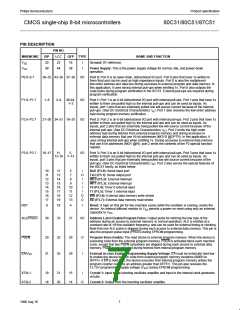
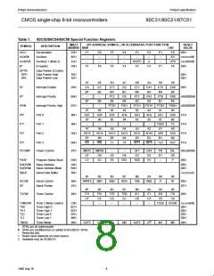
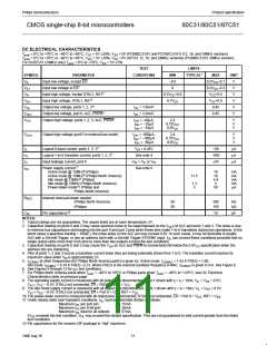
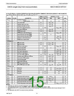
DC ELECTRICAL CHARACTERISTICS
T
amb
= 0°C to +70°C or –40°C to +85°C, V = 5V ±20%, V = 0V (PCB80C31/51 and PCF80C31/51) (12, 16, and 24MHz versions)
CC SS
T
amb
= 0°C to +70°C or –40°C to +85°C, V = 5V ±10%, V = 0V (87C51 12, 16, and 24MHz versions) (PCB80C31/51 33MHz version);
CC SS
For SC87C51 (33MHz only) T
= 0°C to +70°C, V = 5V ±5%
amb
CC
TEST
LIMITS
1
SYMBOL
PARAMETER
CONDITIONS
MIN
–0.5
0
TYPICAL
MAX
0.2V –0.1
UNIT
V
7
V
V
V
V
V
V
V
Input low voltage, except EA
IL
CC
7
Input low voltage to EA
0.2V –0.3
V
IL1
IH
CC
7
Input high voltage, except XTAL1, RST
0.2V +0.9
V
+0.5
+0.5
V
CC
CC
CC
7
Input high voltage, XTAL1, RST
0.7V
V
V
IH1
OL
OL1
OH
CC
11
2
Output low voltage, ports 1, 2, 3
I
I
I
= 1.6mA
0.45
0.45
V
OL
OL
OH
11
2
Output low voltage, port 0, ALE, PSEN
= 3.2mA
V
3
Output high voltage, ports 1, 2, 3, ALE, PSEN
= –60µA,
= –25µA
= –10µA
2.4
V
V
V
I
I
0.75V
OH
OH
CC
CC
0.9V
V
OH1
Output high voltage (port 0 in external bus mode)
I
I
= –800µA,
= –300µA
2.4
V
V
V
OH
OH
I
0.75V
CC
CC
= –80µA
0.9V
OH
7
I
I
I
I
Logical 0 input current, ports 1, 2, 3
V
= 0.45V
–50
–650
±10
µA
µA
µA
IL
IN
7
Logical 1-to-0 transition current, ports 1, 2, 3
See note 4
= V or V
IH
TL
LI
Input leakage current, port 0
V
IN
IL
7
Power supply current:
See note 6
CC
8
5
Active mode @ 12MHz (Philips)
Active mode @ 12MHz (Philips North America)
18
19
4.4
4
mA
mA
mA
mA
µA
11.5
9
Idle mode @ 12MHz (Philips)
Idle mode @ 12MHz (Philips North America)
Power-down mode (Philips and
1.3
3
10
50
Philips North America)
R
C
Internal reset pull-down resistor
(Philips North America)
RST
IO
50
50
300
150
kΩ
kΩ
(Philips)
12
Pin capacitance
10
pF
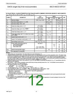
NOTES:
1. Typical ratings are not guaranteed. The values listed are at room temperature, 5V.
2. Capacitive loading on ports 0 and 2 may cause spurious noise to be superimposed on the V s of ALE and ports 1 and 3. The noise is due
OL
to external bus capacitance discharging into the port 0 and port 2 pins when these pins make 1-to-0 transitions during bus operations. In the
worst cases (capacitive loading > 100pF), the noise pulse on the ALE pin may exceed 0.8V. In such cases, it may be desirable to qualify
ALE with a Schmitt Trigger, or use an address latch with a Schmitt Trigger STROBE input. I can exceed these conditions provided that no
OL
single output sinks more than 5mA and no more than two outputs exceed the test conditions.
3. Capacitive loading on ports 0 and 2 may cause the V on ALE and PSEN to momentarily fall below the 0.9V specification when the
OH
CC
address bits are stabilizing.
4. Pins of ports 1, 2 and 3 source a transition current when they are being externally driven from 1 to 0. The transition current reaches its
maximum value when V is approximately 2V.
IN
5. I
at other frequencies (for Philips North America parts) is given by: Active mode: I
= 1.43 X FREQ + 1.90;
CCMAX
CCMAX
Idle mode: I
= 0.14 X FREQ +2.31, where FREQ is the external oscillator frequency in MHz. I
is given in mA. See Figure 8.
CCMAX
CCMAX
6. See Figures 9 through 12 for I test conditions.
CC
7. For Philips North America parts when T
= –40°C to +85°C or Philips parts when T
= –40°C to +125°C, see DC Electrical
amb
amb
Characteristics table on previous page.
8. The operating supply current is measured with all output pins disconnected; XTAL1 driven with t = t = 10ns; V = V + 0.5V;
r
f
IL
SS
V
IH
= V – 0.5V; XTAL2 not connected; EA = RST = Port 0 = V
.
CC
CC
9. The idle mode supply current is measured with all output pins disconnected; XTAL1 driven with t = t = 10ns; V = V + 0.5V;
r
f
IL
SS
V
IH
= V – 0.5V; XTAL2 not connected; EA = Port 0 = V ; RST = V
CC CC SS.
10.The power-down current is measured with all output pins disconnected, XTAL2 not connected, EA = Port 0 = V ; RST = V
CC
SS.
11. Under steady state (non-transient) conditions, I must be externally limited as follows:
OL
Maximum I per port pin:
15mA
26mA
67mA
OL
Maximum I per 8-bit port:
Maximum I total for all outputs:
OL
OL
If I exceeds the test condition, V may exceed the related specification. Pins are not guaranteed to sink current greater than the listed
OL
OL
test conditions.
12.Pin capacitance for the ceramic DIP package is 15pF maximum.
1996 Aug 16
11

 NXP [ NXP ]