Philips Semiconductors
Product specification
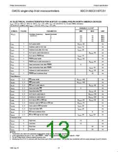
CMOS single-chip 8-bit microcontrollers
80C31/80C51/87C51
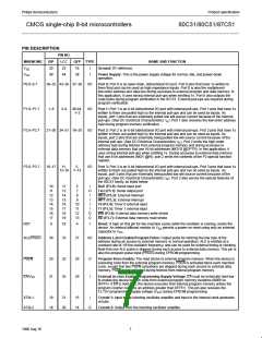
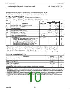
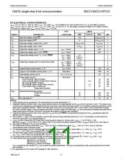
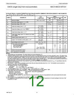
OSCILLATOR CHARACTERISTICS
IDLE MODE
XTAL1 and XTAL2 are the input and output, respectively, of an
inverting amplifier. The pins can be configured for use as an on-chip
oscillator, as shown in the logic symbol.
In idle mode, the CPU puts itself to sleep while all of the on-chip
peripherals stay active. The instruction to invoke the idle mode is the
last instruction executed in the normal operating mode before the
idle mode is activated. The CPU contents, the on-chip RAM, and all
of the special function registers remain intact during this mode. The
idle mode can be terminated either by any enabled interrupt (at
which time the process is picked up at the interrupt service routine
and continued), or by a hardware reset which starts the processor in
the same manner as a power-on reset.
To drive the device from an external clock source, XTAL1 should be
driven while XTAL2 is left unconnected. There are no requirements
on the duty cycle of the external clock signal, because the input to
the internal clock circuitry is through a divide-by-two flip-flop.
However, minimum and maximum high and low times specified in
the data sheet must be observed.
POWER-DOWN MODE
RESET
In the power-down mode, the oscillator is stopped and the
instruction to invoke power-down is the last instruction executed.
Only the contents of the on-chip RAM are preserved. A hardware
reset is the only way to terminate the power-down mode. the control
bits for the reduced power modes are in the special function register
PCON.
A reset is accomplished by holding the RST pin high for at least two
machine cycles (24 oscillator periods), while the oscillator is running.
To insure a good power-up reset, the RST pin must be high long
enough to allow the oscillator time to start up (normally a few
milliseconds) plus two machine cycles.
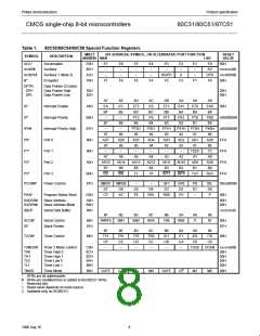
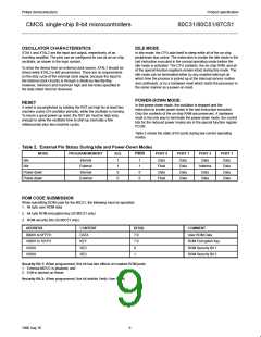
Table 2 shows the state of I/O ports during low current operating
modes.
Table 2. External Pin Status During Idle and Power-Down Modes
MODE
PROGRAM MEMORY
Internal
ALE
PSEN
PORT 0
Data
PORT 1
Data
PORT 2
Data
PORT 3
Data
Idle
Idle
1
1
0
0
1
1
0
0
External
Float
Data
Address
Data
Data
Power-down
Power-down
Internal
Data
Data
Data
External
Float
Data
Data
Data
ROM CODE SUBMISSION
When submitting ROM code for the 80C51, the following must be specified:
1. 4k byte user ROM data
2. 64 byte ROM encryption key (SC80C51 only)
3. ROM security bits (SC80C51 only).
ADDRESS
0000H to 0FFFH
1000H to 101FH
1020H
CONTENT
DATA
KEY
BIT(S)
7:0
7:0
0
COMMENT
User ROM Data
ROM Encryption Key
ROM Security Bit 1
ROM Security Bit 2
SEC
1020H
SEC
1
Security Bit 1: When programmed, this bit has two effects on masked ROM parts:
1. External MOVC is disabled, and
2. EA# is latched on Reset.
Security Bit 2: When programmed, this bit inhibits Verify User ROM.
9
1996 Aug 16

 NXP [ NXP ]