Philips Semiconductors
Product specification
CMOS single-chip 8-bit microcontrollers
80C31/80C51/87C51
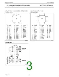
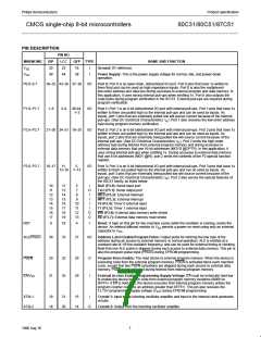
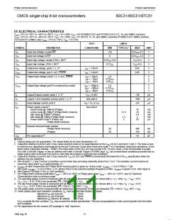
PIN DESCRIPTION
PIN NO.
MNEMONIC
DIP
20
LCC
22
QFP TYPE
NAME AND FUNCTION
V
V
16
38
I
I
Ground: 0V reference.
SS
40
44
Power Supply: This is the power supply voltage for normal, idle, and power-down
CC
operation.
P0.0–0.7
39–32 43–36 37–30
I/O
Port 0: Port 0 is an open-drain, bidirectional I/O port. Port 0 pins that have 1s written to
them float and can be used as high-impedance inputs. Port 0 is also the multiplexed
low-order address and data bus during accesses to external program and data memory. In
this application, it uses strong internal pull-ups when emitting 1s. Port 0 also outputs the
code bytes during program verification in the 87C51. External pull-ups are required during
program verification.
P1.0–P1.7
P2.0–P2.7
1–8
2–9
40-44,
1–3
I/O
I/O
Port 1: Port 1 is an 8-bit bidirectional I/O port with internal pull-ups. Port 1 pins that have 1s
written to them are pulled high by the internal pull-ups and can be used as inputs. As
inputs, port 1 pins that are externally pulled low will source current because of the internal
pull-ups. (See DC Electrical Characteristics: I ). Port 1 also receives the low-order address
IL
byte during program memory verification.
21–28 24–31 18–25
Port 2: Port 2 is an 8-bit bidirectional I/O port with internal pull-ups. Port 2 pins that have 1s
written to them are pulled high by the internal pull-ups and can be used as inputs. As
inputs, port 2 pins that are externally being pulled low will source current because of the
internal pull-ups. (See DC Electrical Characteristics: I ). Port 2 emits the high-order
IL
address byte during fetches from external program memory and during accesses to
external data memory that use 16-bit addresses (MOVX @DPTR). In this application, it
uses strong internal pull-ups when emitting 1s. During accesses to external data memory
that use 8-bit addresses (MOV @Ri), port 2 emits the contents of the P2 special function
register.
P3.0–P3.7
10–17
11,
5,
I/O
Port 3: Port 3 is an 8-bit bidirectional I/O port with internal pull-ups. Port 3 pins that have 1s
written to them are pulled high by the internal pull-ups and can be used as inputs. As
inputs, port 3 pins that are externally being pulled low will source current because of the
13–19 7–13
pull-ups. (See DC Electrical Characteristics: I ). Port 3 also serves the special features of
IL
the 80C51 family, as listed below:
10
11
12
13
14
15
16
17
11
13
14
15
16
17
18
19
5
7
8
I
O
I
I
I
I
O
O
RxD (P3.0): Serial input port
TxD (P3.1): Serial output port
INT0 (P3.2): External interrupt
INT1 (P3.3): External interrupt
T0 (P3.4): Timer 0 external input
T1 (P3.5): Timer 1 external input
WR (P3.6): External data memory write strobe
RD (P3.7): External data memory read strobe
9
10
11
12
13
RST
9
10
4
I
Reset: A high on this pin for two machine cycles while the oscillator is running, resets the
device. An internal diffused resistor to V permits a power-on reset using only an external
SS
capacitor to V
.
CC
ALE/PROG
30
33
27
I/O
Address Latch Enable/Program Pulse: Output pulse for latching the low byte of the
address during an access to external memory. In normal operation, ALE is emitted at a
constant rate of 1/6 the oscillator frequency, and can be used for external timing or clocking.
Note that one ALE pulse is skipped during each access to external data memory. This pin is
also the program pulse input (PROG) during EPROM programming.
PSEN
29
31
32
35
26
29
O
I
Program Store Enable: The read strobe to external program memory. When the device is
executing code from the external program memory, PSEN is activated twice each machine
cycle, except that two PSEN activations are skipped during each access to external data
memory. PSEN is not activated during fetches from internal program memory.
EA/V
External Access Enable/Programming Supply Voltage: EA must be externally held low
to enable the device to fetch code from external program memory locations 0000H to
0FFFH. If EA is held high, the device executes from internal program memory unless the
program counter contains an address greater than 0FFFH. This pin also receives the
PP
12.75V programming supply voltage (V ) during EPROM programming.
PP
XTAL1
XTAL2
19
18
21
20
15
14
I
Crystal 1: Input to the inverting oscillator amplifier and input to the internal clock generator
circuits.
O
Crystal 2: Output from the inverting oscillator amplifier.
7
1996 Aug 16

 NXP [ NXP ]