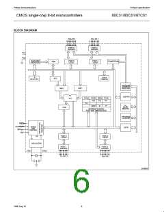
Philips Semiconductors
Product specification
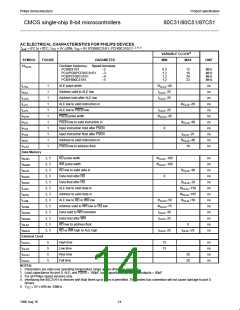
CMOS single-chip 8-bit microcontrollers
80C31/80C51/87C51
Electrical Deviations from Commercial Specifications for Extended Temperature Range (87C51)
DC and AC parameters not included here are the same as in the commercial temperature range table.
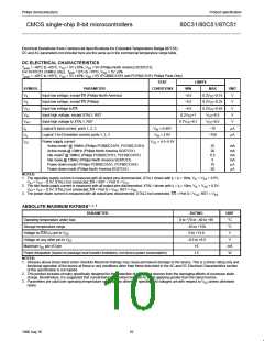
DC ELECTRICAL CHARACTERISTICS
T
amb
= –40°C to +85°C, V = 5V ±10%, V = 0V (Philips North America SC87C51);
CC SS
For SC87C51 (33MHz only), T
= 0°C to +70°C, V = 5V ±5%
CC
amb
T
amb
= –40°C to +85°C, V = 5V ±10%, V = 0V (PCB80C31/51 and PCF80C31/51 Philips Parts Only)
CC SS
TEST
LIMITS
SYMBOL
PARAMETER
CONDITIONS
MIN
–0.5
–0.5
–0.5
MAX
0.2V –0.15
UNIT
V
V
V
V
V
V
Input low voltage, except EA (Philips North America)
Input low voltage, except EA (Philips)
Input low voltage to EA
IL
CC
0.2V –0.25
V
IL
CC
0.2V –0.45
V
IL1
IH
CC
Input high voltage, except XTAL1, RST
Input high voltage to XTAL1, RST
Logical 0 input current, ports 1, 2, 3
Logical 1-to-0 transition current, ports 1, 2, 3
Power supply current:
0.2V +1
V
CC
V
CC
+0.5
+0.5
V
CC
0.7V +0.1
V
IH1
CC
I
I
I
V
= 0.45V
= 2.0V
IN
–75
µA
µA
IL
IN
V
–750
TL
V
CC
= 4.5–5.5V
CC
1
Active mode @ 16MHz (Philips PCB80C31/51, PCF80C31/51)
Active mode @ 12MHz (Philips North America SC87C51)
Idle mode @ 16MHz (Philips PCB80C31/51, PCF80C31/51)
Idle mode @ 12MHz (Philips North America SC87C51)
Power-down mode (Philips PCB80C31/51, PCF80C31/51)
Power-down mode (Philips North America SC87C51)
25
20
6.5
5
75
50
mA
mA
mA
mA
µA
2
3
µA
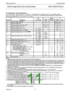
NOTES:
1. The operating supply current is measured with all output pins disconnected; XTAL1 driven with t = t = 10ns; V = V + 0.5V;
r
f
IL
SS
V
IH
= V – 0.5V; XTAL2 not connected; EA = RST = Port 0 = V
.
CC
CC
2. The idle mode supply current is measured with all output pins disconnected; XTAL1 driven with t = t = 10ns; V = V + 0.5V;
r
f
IL
SS
V
IH
= V – 0.5V; XTAL2 not connected; EA = Port 0 = V ; RST = V
CC CC SS.
3. The power-down current is measured with all output pins disconnected, XTAL2 not connected, EA = Port 0 = V ; RST = V
CC
SS.
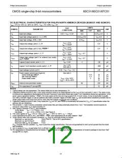
ABSOLUTE MAXIMUM RATINGS1, 2, 3
PARAMETER
RATING
0 to +70 or –40 to +85
–65 to +150
0 to +13.0
–0.5 to +6.5
15
UNIT
Operating temperature under bias
Storage temperature range
°C
°C
V
Voltage on EA/V pin to V
PP
SS
Voltage on any other pin to V
V
SS
Maximum I per I/O pin
mA
W
OL
Power dissipation (based on package heat transfer limitations, not device power consumption)
1.5
NOTES:
1. Stresses above those listed under Absolute Maximum Ratings may cause permanent damage to the device. This is a stress rating only and
functional operation of the device at these or any conditions other than those described in the AC and DC Electrical Characteristics section
of this specification is not implied.
2. This product includes circuitry specifically designed for the protection of its internal devices from the damaging effects of excessive static
charge. Nonetheless, it is suggested that conventional precautions be taken to avoid applying greater than the rated maxima.
3. Parameters are valid over operating temperature range unless otherwise specified. All voltages are with respect to V unless otherwise
SS
noted.
10
1996 Aug 16

 NXP [ NXP ]