Philips Semiconductors
Product specification
Multimedia bridge, high performance
Scaler and PCI circuit (SPCI)
SAA7146A
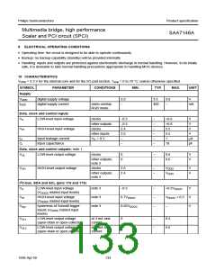
SYMBOL
PARAMETER
CONDITIONS
note 4
MIN.
TYP.
MAX.
UNIT
to(f)
output fall time from VIHmin to
VILmax with a bus capacitance
from 10 to 400 pF
V
up to 3 mA sink
current at VOL1
20 + 0.1Cb
−
250
250
up to 3 mA sink
current at VOL2
20 + 0.1Cb
−
−
Ii
input current each I/O pin with an note 3
input voltage between 0.4 and
0.9VDDi2Cmax
−10(5)
+10(5)
µA
Ci
capacitance for each I/O pin
−
−
−
10
45
pF
ns
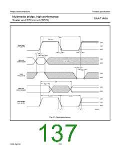
Clock input timing (LLC_A and LLC_B); see Fig.47
tLLC_A
,
cycle time
31
tLLC_B
δ
tr
tf
duty factor
rise time
fall time
tLLCH/tLLC
40
−
50
−
60
5
%
ns
ns
−
−
6
Data and control input timing; see Fig.47
tSU
tHD
set-up time
hold time
6
3
−
−
−
−
ns
ns
Clock output timing (LLC_A, LLC_B); see Fig.47
CL
output load capacitance
cycle time
15
31
−
−
40
45
pF
ns
tLLC_A
,
tLLC_B
δ
tr
tf
duty factor
rise time
fall time
tLLCH/tLLC
40
−
50
−
60
5
%
0.6 to 2.6 V
2.6 to 0.6 V
ns
ns
−
−
5
Data and control output timing; see Fig.47
CL
tOH
tpd
load capacitance
output hold time
15
4
−
−
−
40
−
pF
ns
ns
CL = 15 pF
CL = 40 pF
propagation delay from positive
edge of LLC_A, LLC_B
−
25
PCI I/O signals
DC SPECIFICATION
VIH
VIL
HIGH-level input voltage
LOW-level input voltage
2.0
−0.5
−
−
−
−
−
−
−
5.75
+0.8
70
V
V
ILIH
ILIL
HIGH-level input leakage current VI = 2.7 V; note 1
LOW-level input leakage current VI = 0.5 V; note 1
µA
µA
V
−
−70
−
VOH
VOL
HIGH-level output voltage
LOW-level output voltage
IO = −2 mA
2.4
−
IO = 3 and 6 mA;
note 6
0.55
V
1998 Apr 09
134

 NXP [ NXP ]