Philips Semiconductors
Product specification
Radio tuning PLL frequency synthesizer
SAA1057
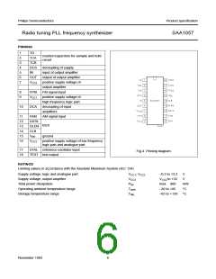
PINNING
1
2
3
4
5
6
7
TR
resistor/capacitors for sample and hold
circuit
TCA
TCB
DCS
IN
decoupling of supply
input of output amplifier
output of output amplifier
positive supply voltage of
output amplifier
OUT
VCC3
8
9
FFM
VCC1
FM signal input
positive supply voltage of
high frequency logic part
decoupling of input
amplifiers
10
DCA
11
12
13
14
15
16
FAM
DATA
DLEN
CLB
AM signal input
BUS
VEE
ground
VCC2
positive supply voltage of low frequency
logic part and analogue part
17
18
XTAL reference oscillator input
TEST test output
Fig.4 Pinning diagram.
RATINGS
Limiting values in accordance with the Absolute Maximum System (IEC 134)
Supply voltage; logic and analogue part
Supply voltage; output amplifier
Total power dissipation
V
CC1; VCC2
−0,3 to 13,2
VCC2 to +32
max. 800
−30 to +85
V
VCC3
Ptot
V
mW
°C
Operating ambient temperature range
Storage temperature range
Tamb
Tstg
−65 to +150 °C
November 1983
6

 NXP [ NXP ]