Philips Semiconductors
Product specification
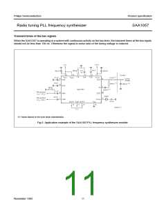
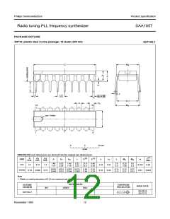
Radio tuning PLL frequency synthesizer
SAA1057
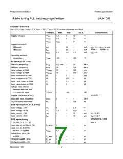
SYMBOL
MIN.
TYP.
MAX.
CONDITIONS
Set-up time for DATA
to CLB
tDATAlead
tDATAhold
tDLENhold
2
0
2
−
−
−
−
µs
µs
µs
Hold time for DATA to CLB
Hold time for DLEN to CLB
Set-up time for DLEN to
CLB load pulse
−
−
tCLBlag2
2
5
−
−
−
−
µs
µs
Busy time from load pulse
to next start of transmission
Busy time
next transmission after
word ‘B’ to other device
tDIST
or
asynchronous mode
synchronous mode
tDIST
tDIST
0,3
1,3
−
−
−
−
ms
ms
next transmission to
SAA1057 after word
‘A’ (see also note 5)
Sample and hold circuit
(TR, TCA, TCB)
see also notes 3; 4
Minimum output voltage
VTCA
VTCB
,
,
−
−
1,3
−
V
V
Maximum output voltage
VTCA
VTCB
−
V
CC2−0,7
Capacitance at TCA
(external)
CTCA
CTCA
tdis
−
−
−
−
−
−
2,2
2,7
5
nF
nF
µs
µs
Ω
REFH = ‘1’
REFH = ‘0’
REFH = ‘1’
REFH = ‘0’
external
−
Discharge time at TCA
−
tdis
−
6,25
−
Resistance at TR
Voltage at TR during
discharge
RTR
100
VTR
−
−
−
0,7
−
−
V
Capacitance at TCB
Bias current into TCA, TCB
CTCB
Ibias
10
10
nF
nA
external
in-lock
−
Programmable current amplifier
(PCA)
Output current of the
dig. phase detector
± Idig
−
0,4
−
mA
Current gain of PCA
CP3 CP2 CP1 CP0
P1
P2
P3
P4
P5
0
0
0
0
1
0
0
0
1
1
0
0
1
1
1
0
1
0
0
0
GP1
GP2
GP3
GP4
GP5
−
−
−
−
−
0,023
0,07
0,23
0,7
−
−
−
−
−
VCC2 ≥ 5 V (only for P1)
2,3
November 1983
8

 NXP [ NXP ]