PHP78NQ03LT
Philips Semiconductors
N-channel TrenchMOS logic level FET
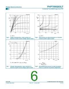
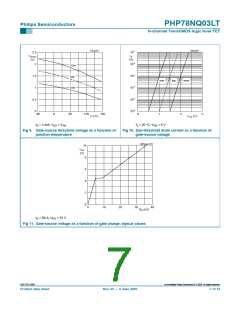
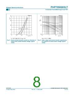
6. Characteristics
Table 5:
Characteristics
Tj = 25 °C unless otherwise specified.
Symbol Parameter
Conditions
Min
Typ
Max Unit
Static characteristics
V(BR)DSS drain-source breakdown voltage
ID = 250 µA; VGS = 0 V
Tj = 25 °C
25
22
-
-
-
-
V
V
Tj = −55 °C
VGS(th)
gate-source threshold voltage
drain-source leakage current
ID = 1 mA; VDS = VGS; Figure 9 and 10
Tj = 25 °C
1
1.5
2
V
V
V
Tj = 175 °C
0.5
-
-
-
-
Tj = −55 °C
2.2
IDSS
VDS = 25 V; VGS = 0 V
Tj = 25 °C
-
-
-
-
10
µA
µA
nA
Tj = 150 °C
-
500
100
IGSS
gate-source leakage current
VGS = ±15 V; VDS = 0 V
VGS = 5 V; ID = 25 A; Figure 6 and 8
Tj = 25 °C
10
RDSon
drain-source on-state resistance
-
-
-
11.5 13.5 mΩ
20.7 24.3 mΩ
Tj = 175 °C
VGS = 10 V; ID = 25 A; Figure 6 and 8
7.65
9
mΩ
Dynamic characteristics
QG(tot)
QGS
QGD
Ciss
Coss
Crss
td(on)
tr
total gate charge
gate-source charge
gate-drain (Miller) charge
input capacitance
output capacitance
reverse transfer capacitance
turn-on delay time
rise time
ID = 50 A; VDS = 15 V; VGS = 5 V;
Figure 11
-
-
-
-
-
-
-
-
-
-
13
-
nC
nC
nC
pF
pF
pF
ns
ns
ns
ns
4.8
4.2
1074
389
156
20
-
5.6
-
VGS = 0 V; VDS = 25 V; f = 1 MHz;
Figure 13
-
-
VDS = 15 V; RL = 0.6 Ω; VGS = 10 V;
RG = 5.6 Ω
33
130
48
60
92
td(off)
tf
turn-off delay time
fall time
30
40
Source-drain diode
VSD
trr
source-drain (diode forward) voltage IS = 25 A; VGS = 0 V; Figure 12
-
-
-
0.95 1.2
V
reverse recovery time
recovered charge
IS = 20 A; dIS/dt = −100 A/µs; VGS = 0 V;
VR = 25 V
40
32
-
-
ns
nC
Qr
9397 750 15086
© Koninklijke Philips Electronics N.V. 2005. All rights reserved.
Product data sheet
Rev. 05 — 9 June 2005
5 of 12

 NXP [ NXP ]