PDIUSBD12
USB interface device with parallel bus
Philips Semiconductors
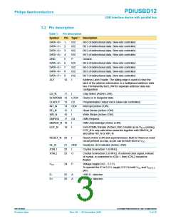
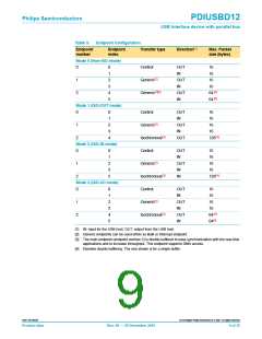
Table 1:
Pin description…continued
Symbol
Pin Type[1] Description
VOUT3.3
27
P
3.3 V regulated output. To operate the IC at 3.3 V, supply a
3.3 V to both VCC and VOUT3.3 pins.
A0
28
I
Address bit. A0 = 1 selects command instruction; A0 = 0 selects
the data phase. This bit is a don’t care in a multiplexed address
and data bus configuration and should be tied HIGH.
[1] O2: Output with 2 mA drive
OD4: Output Open Drain with 4 mA drive
OD8: Output Open Drain with 8 mA drive
IO2: Input and Output with 2 mA drive
O4: Output with 4 mA drive.
4. Ordering information
Table 2:
Ordering information
Temperature range
Packages
Outside North America
North America
Pkg. Dwg. #
28-pin plastic SO
−40 °C to +85 °C
−40 °C to +85 °C
PDIUSBD12 D
PDIUSBD12 D
SOT136-1
28-pin plastic TSSOP
PDIUSBD12 PW
PDIUSBD12PW DH SOT361-1
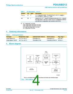
5. Block diagram
This is a conceptual block diagram and does not include each individual signal.
Fig 2. Block diagram.
9397 750 09238
© Koninklijke Philips Electronics N.V. 2001. All rights reserved.
Product data
Rev. 08 — 20 December 2001
4 of 35

 NXP [ NXP ]