PDIUSBD12
USB interface device with parallel bus
Philips Semiconductors
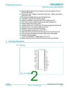
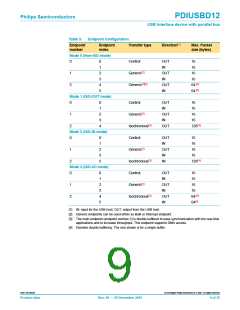
3.2 Pin description
Table 1:
Symbol
DATA <0>
DATA <1>
DATA <2>
DATA <3>
GND
Pin description
Pin Type[1] Description
1
2
3
4
5
6
7
8
9
10
IO2
IO2
IO2
IO2
P
Bit 0 of bidirectional data. Slew-rate controlled.
Bit 1 of bidirectional data. Slew-rate controlled.
Bit 2 of bidirectional data. Slew-rate controlled.
Bit 3 of bidirectional data. Slew-rate controlled.
Ground.
DATA <4>
DATA <5>
DATA <6>
DATA <7>
ALE
IO2
IO2
IO2
IO2
I
Bit 4 of bidirectional data. Slew-rate controlled.
Bit 5 of bidirectional data. Slew-rate controlled.
Bit 6 of bidirectional data. Slew-rate controlled.
Bit 7 of bidirectional data. Slew-rate controlled.
Address Latch Enable. The falling edge is used to close the
latch of the address information in a multiplexed address/ data
bus. Permanently tied LOW for separate address/ data bus
configuration.
CS_N
11
I
Chip Select (Active LOW).
Device is in Suspend state.
Programmable Output Clock (slew-rate controlled).
Interrupt (Active LOW).
SUSPEND 12
I,OD4
CLKOUT
INT_N
13
14
15
16
17
O2
OD4
RD_N
I
Read Strobe (Active LOW).
Write Strobe (Active LOW).
DMA Request.
WR_N
I
DMREQ
O4
DMACK_N 18
EOT_N 19
I
I
DMA Acknowledge (Active LOW).
End of DMA Transfer (Active LOW). Double up as VBUS sensing.
EOT_N is only valid when asserted together with DMACK_N
and either RD_N or WR_N.
RESET_N 20
I
Reset (Active LOW and asynchronous). Built-in Power-on reset
circuit present on chip, so pin can be tied HIGH to VCC
GoodLink LED indicator (Active LOW)
Crystal Connection 1 (6 MHz).
.
GL_N
XTAL1
XTAL2
21
22
23
OD8
I
O
Crystal Connection 2 (6 MHz). If external clock signal, instead
of crystal, is connected to XTAL1, then XTAL2 should be
floated.
VCC
24
P
Voltage supply (4.0 − 5.5 V).
To operate the IC at 3.3 V, supply 3.3 V to both VCC and VOUT3.3
pins.
D−
25
26
A
A
USB D− data line.
D+
USB D+ data line.
9397 750 09238
© Koninklijke Philips Electronics N.V. 2001. All rights reserved.
Product data
Rev. 08 — 20 December 2001
3 of 35

 NXP [ NXP ]