PDIUSBD12
USB interface device with parallel bus
Philips Semiconductors
PDIUSBD12
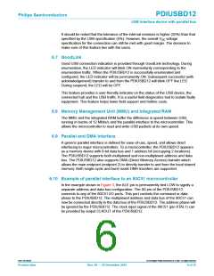
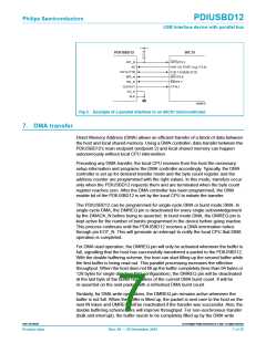
80C51
INT_N
A0
INTO/P3.2
ANY I/O PORT (e.g. P3.3)
[
]
[
]
[
]
DATA 7:0
P 0.7:0.0 /AD 7:0
WR_N
RD_N
WR/P3.6
RD/P3.7
CLKOUT
CS_N
XTAL1
ALE
SV00870
Fig 3. Example of a parallel interface to an 80C51 microcontroller.
7. DMA transfer
Direct Memory Address (DMA) allows an efficient transfer of a block of data between
the host and local shared memory. Using a DMA controller, data transfer between the
PDIUSBD12’s main endpoint (endpoint 2) and local shared memory can happen
autonomously without local CPU intervention.
Preceding any DMA transfer, the local CPU receives from the host the necessary
setup information and programs the DMA controller accordingly. Typically, the DMA
controller is set up for demand transfer mode and the byte count register and the
address counter are programmed with the right values. In this mode, transfers occur
only when the PDIUSBD12 requests them and are terminated when the byte count
register reaches zero. After the DMA controller has been programmed, the DMA
enable bit of the PDIUSBD12 is set by the local CPU to initiate the transfer.
The PDIUSBD12 can be programmed for single-cycle DMA or burst mode DMA. In
single-cycle DMA, the DMREQ pin is deactivated for every single acknowledgement
by the DMACK_N before being re-asserted. In burst mode DMA, the DMREQ pin is
kept active for the number of bursts programmed in the device before going inactive.
This process continues until the PDIUSBD12 receives a DMA termination notice
through pin EOT_N. This will generate an interrupt to notify the local CPU that DMA
operation is completed.
For DMA read operation, the DMREQ pin will only be activated whenever the buffer is
full, signalling that the host has successfully transferred a packet to the PDIUSBD12.
With the double buffering scheme, the host can start filling up the second buffer while
the first buffer is being read out. This parallel processing increases the effective
throughput. When the host does not fill up the buffer completely (less than 64 bytes or
128 bytes for single direction ISO configuration), the DMREQ pin will be deactivated
at the last byte of the buffer regardless of the current DMA burst count. It will be
re-asserted on the next packet with a refreshed DMA burst count.
Similarly, for DMA write operations, the DMREQ pin remains active whenever the
buffer is not full. When the buffer is filled up, the packet is sent over to the host on the
next IN token and DMREQ will be reactivated if the transfer was successful. Also, the
double buffering scheme here will improve throughput. For non-isochronous transfer
(bulk and interrupt), the buffer needs to be completely filled up by the DMA write
9397 750 09238
© Koninklijke Philips Electronics N.V. 2001. All rights reserved.
Product data
Rev. 08 — 20 December 2001
7 of 35

 NXP [ NXP ]