Philips Semiconductors
Preliminary data
Low power, low price, low pin count (20 pin)
microcontroller with 4 kbyte OTP
87LPC764
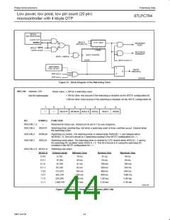
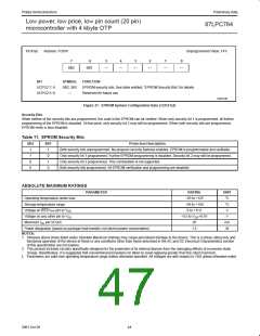
UCFG2
Address: FD01h
Unprogrammed Value: FFh
7
6
5
4
3
2
1
0
SB2
SB1
—
—
—
—
—
—
BIT
SYMBOL
SB2, SB1
—
FUNCTION
UCFG2.7, 6
UCFG2.5–0
EPROM security bits. See table entitled, “EPROM Security Bits” for details.
Reserved for future use.
SU01186
Figure 37. EPROM System Configuration Byte 2 (UCFG2)
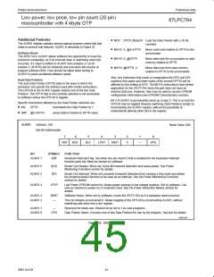
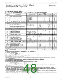
Security Bits
When neither of the security bits are programmed, the code in the EPROM can be verified. When only security bit 1 is programmed, all further
programming of the EPROM is disabled. At that point, only security bit 2 may still be programmed. When both security bits are programmed,
EPROM verify is also disabled.
Table 11. EPROM Security Bits
SB2
SB1
Protection Description
1
1
0
0
1
0
1
0
Both security bits unprogrammed. No program security features enabled. EPROM is programmable and verifiable.
Only security bit 1 programmed. Further EPROM programming is disabled. Security bit 2 may still be programmed.
Only security bit 2 programmed. This combination is not supported.
Both security bits programmed. All EPROM verification and programming are disabled.
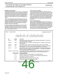
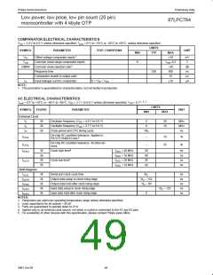
ABSOLUTE MAXIMUM RATINGS
PARAMETER
RATING
–55 to +125
–65 to +150
0 to +11.0
UNIT
°C
°C
V
Operating temperature under bias
Storage temperature range
Voltage on RST/V pin to V
PP
SS
Voltage on any other pin to V
–0.5 to V +0.5V
V
SS
DD
Maximum I per I/O pin
20
mA
W
OL
Power dissipation (based on package heat transfer, not device power consumption)
1.5
NOTES:
1. Stresses above those listed under Absolute Maximum Ratings may cause permanent damage to the device. This is a stress rating only and
functional operation of the device at these or any conditions other than those described in the AC and DC Electrical Characteristics section
of this specification are not implied.
2. This product includes circuitry specifically designed for the protection of its internal devices from the damaging effects of excessive static
charge. Nonetheless, it is suggested that conventional precautions be taken to avoid applying greater than the rated maximum.
3. Parameters are valid over operating temperature range unless otherwise specified. All voltages are with respect to VSS unless otherwise noted.
44
2001 Oct 26

 NXP [ NXP ]