Philips Semiconductors
Preliminary data
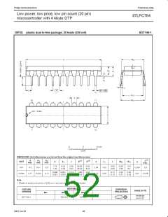
Low power, low price, low pin count (20 pin)
microcontroller with 4 kbyte OTP
87LPC764
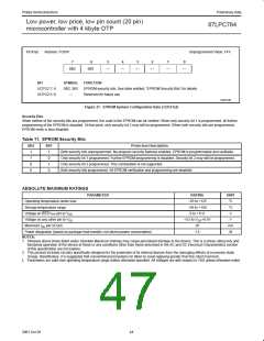
DC ELECTRICAL CHARACTERISTICS
V
= 2.7 V to 6.0 V unless otherwise specified; T
= 0°C to +70°C or –40°C to +85°C, unless otherwise specified.
DD
amb
LIMITS
SYMBOL
PARAMETER
Power supply current, operating
Power supply current, Idle mode
TEST CONDITIONS
UNIT
MAX
1
MIN
TYP
15
4
11
11
11
11
5.0 V, 20 MHz
3.0 V, 10 MHz
5.0 V, 20 MHz
3.0 V, 10 MHz
25
7
mA
mA
mA
mA
µA
µA
V
I
DD
6
10
4
I
ID
2
11
5.0 V
1
10
5
I
Power supply current, Power Down mode
RAM keep-alive voltage
PD
11
3.0 V
1
V
RAM
1.5
4.0 V < V < 6.0 V
–0.5
–0.5
–0.5
0.2 V –0.1
V
DD
DD
V
Input low voltage (TTL input)
IL
2.7 V < V < 4.0 V
0.7
V
DD
V
IL1
Negative going threshold (Schmitt input)
Input high voltage (TTL input)
Positive going threshold (Schmitt input)
Hysteresis voltage
0.3 V
V
DD
V
IH
0.2 V +0.9
V
DD
V
DD
+0.5
+0.5
V
DD
V
IH1
0.7 V
V
DD
HYS
0.2 V
V
DD
5, 9
V
Output low voltage all ports
I
I
I
I
I
= 3.2 mA, V = 2.7 V
0.4
V
OL
OL
OL
OH
OH
OH
DD
5, 9
V
OL1
Output low voltage all ports
= 20 mA, V = 2.7 V
1.0
V
DD
= –20 µA, V = 2.7 V
V
DD
V
DD
V
DD
–0.7
–0.7
–0.7
V
DD
3
V
OH
Output high voltage, all ports
= –30 µA, V = 4.5 V
V
DD
4
V
OH1
Output high voltage, all ports
= –1.0 mA, V = 2.7 V
V
DD
10
C
Input/Output pin capacitance
15
–50
±2
pF
µA
µA
µA
µA
kΩ
V
IO
8
I
I
Logical 0 input current, all ports
V
IN
V
IN
V
IN
V
IN
= 0.4 V
IL
7
Input leakage current, all ports
= V or V
IL IH
LI
= 1.5 V at V = 3.0 V
–30
–250
–650
225
2.69
3.99
1.41
DD
3, 6
I
TL
Logical 1 to 0 transition current, all ports
Internal reset pull-up resistor
= 2.0 V at V = 5.5 V
–150
40
DD
R
RST
12
V
Brownout trip voltage with BOV = 1
2.35
3.45
1.11
BOLOW
V
BOHI
Brownout trip voltage with BOV = 0
Reference voltage
V
V
REF
1.26
tbd
V
t
C
(V
)
REF
Temperature coefficient
Supply sensitivity
ppm/°C
%/V
SS
tbd
NOTES:
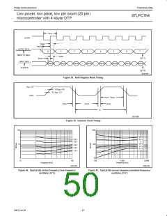
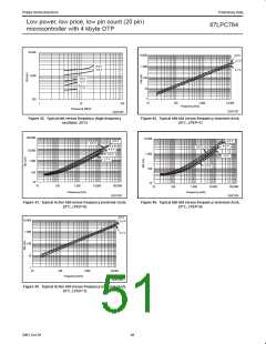
1. Typical ratings are not guaranteed. The values listed are at room temperature, 5 V.
2. See other Figures for details.
Active mode: I
= tbd
= tbd
CC(MAX)
Idle mode: I
CC(MAX)
3. Ports in quasi-bidirectional mode with weak pull-up (applies to all port pins with pull-ups). Does not apply to open drain pins.
4. Ports in PUSH-PULL mode. Does not apply to open drain pins.
5. In all output modes except high impedance mode.
6. Port pins source a transition current when used in quasi-bidirectional mode and externally driven from 1 to 0. This current is highest when
is approximately 2 V.
V
IN
7. Measured with port in high impedance mode. Parameter is guaranteed but not tested at cold temperature.
8. Measured with port in quasi-bidirectional mode.
9. Under steady state (non-transient) conditions, I must be externally limited as follows:
OL
Maximum I per port pin:
20 mA
80 mA
5 mA
OL
Maximum total I for all outputs:
OL
Maximum total I for all outputs:
OH
If I exceeds the test condition, V may exceed the related specification. Pins are not guaranteed to sink current greater than the listed
OL
OL
test conditions.
10.Pin capacitance is characterized but not tested.
11. The I , I , and I specifications are measured using an external clock with the following functions disabled: comparators, brownout
DD ID
PD
detect, and watchdog timer. For V = 3 V, LPEP = 1. Refer to the appropriate figures on the following pages for additional current drawn by
DD
each of these functions and detailed graphs for other frequency and voltage combinations.
12.Devices initially operating at V = 2.7V or above and at f
= 10 MHz or less are guaranteed to continue to execute instructions correctly
DD
OSC
at the brownout trip point. Initial power-on operation below V = 2.7 V is not guaranteed.
DD
13.Devices initially operating at V = 4.0 V or above and at f
= 20 MHz or less are guaranteed to continue to execute instructions correctly
DD
OSC
at the brownout trip point. Initial power-on operation below V = 4.0 V and F
> 10 MHz is not guaranteed.
DD
OSC
45
2001 Oct 26

 NXP [ NXP ]