Philips Semiconductors
Preliminary data
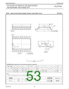
Low power, low price, low pin count (20 pin)
microcontroller with 4 kbyte OTP
87LPC764
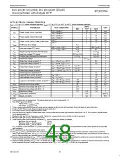
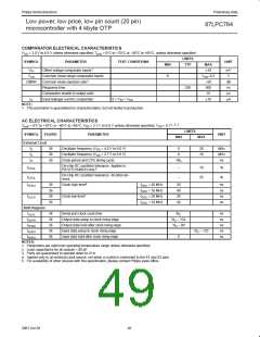
COMPARATOR ELECTRICAL CHARACTERISTICS
V
DD
= 3.0 V to 6.0 V unless otherwise specified; T
= 0°C to +70°C or –40°C to +85°C, unless otherwise specified
amb
LIMITS
SYMBOL
PARAMETER
TEST CONDITIONS
UNIT
MAX
MIN
TYP
1
V
Offset voltage comparator inputs
±10
–0.3
DD
mV
V
IO
V
CR
Common mode range comparator inputs
0
V
1
CMRR
Common mode rejection ratio
–50
500
10
dB
ns
µs
µA
Response time
250
Comparator enable to output valid
Input leakage current, comparator
I
IL
0 < V < V
DD
±10
IN
NOTE:
1. This parameter is guaranteed by characterization, but not tested in production.
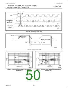
AC ELECTRICAL CHARACTERISTICS
1, 2, 3
T
= 0°C to +70°C or –40°C to +85°C, V = 2.7 V to 6.0 V unless otherwise specified; V = 0 V
amb
DD SS
LIMITS
SYMBOL
FIGURE
PARAMETER
UNIT
MIN
MAX
External Clock
f
C
f
C
t
C
39
39
39
Oscillator frequency (V = 4.0 V to 6.0 V)
0
0
20
10
MHz
MHz
ns
DD
Oscillator frequency (V = 2.7 V to 6.0 V)
DD
Clock period and CPU timing cycle
1/f
C
On-chip RC oscillator tolerance. Applies to
P87LPC764BDH only.
f
f
–
–
10
25
%
%
CTOL
5
On-chip RC oscillator tolerance. All other de-
vices.
CTOL
4
t
39
39
39
39
Clock high-time
f
f
f
f
= 20 MHz
= 10 MHz
= 20 MHz
= 10 MHz
20
ns
ns
ns
ns
CHCX
OSC
OSC
OSC
OSC
40
20
40
4
t
Clock low-time
CLCX
Shift Register
t
38
38
38
38
38
Serial port clock cycle time
6t
ns
ns
ns
ns
ns
XLXL
C
t
t
Output data setup to clock rising edge
Output data hold after clock rising edge
Input data setup to clock rising edge
Input data hold after clock rising edge
5t – 133
C
QVXH
XHQX
1t – 80
C
t
t
5t – 133
C
XHDV
0
XHDX
NOTES:
1. Parameters are valid over operating temperature range unless otherwise specified.
2. Load capacitance for all outputs = 80 pF.
3. Parts are guaranteed to operate down to 0 Hz.
4. Applies only to an external clock source, not when a crystal is connected to the X1 and X2 pins.
5. For availability of other devices with this specification, please contact Philips sales office.
46
2001 Oct 26

 NXP [ NXP ]