Philips Semiconductors
Preliminary data
Low power, low price, low pin count (20 pin)
microcontroller with 4 kbyte OTP
87LPC764
32-Byte Customer Code Space
A small supplemental EPROM space is reserved for use by the
EPROM Characteristics
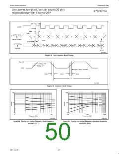
Programming of the EPROM on the 87LPC764 is accomplished with
a serial programming method. Commands, addresses, and data are
transmitted to and from the device on two pins after programming
mode is entered. Serial programming allows easy implementation of
In-System Programming of the 87LPC764 in an application board.
Details of In-System Programming can be found in application note
AN466.
customer in order to identify code revisions, store checksums, add a
serial number to each device, or any other desired use. This area
exists in the code memory space from addresses FCE0h through
FCFFh. Code execution from this space is not supported, but it may
be read as data through the use of the MOVC instruction with the
appropriate addresses. The memory may be programmed at the
same time as the rest of the code memory and UCFG bytes are
programmed.
The 87LPC764 contains three signature bytes that can be read and
used by an EPROM programming system to identify the device. The
signature bytes designate the device as an 87LPC764 manufactured
by Philips. The signature bytes may be read by the user program at
addresses FC30h, FC31h and FC60h with the MOVC instruction,
using the DPTR register for addressing.
System Configuration Bytes
A number of user configurable features of the 87LPC764 must be
defined at power up and therefore cannot be set by the program after
start of execution. Those features are configured through the use of
two EPROM bytes that are programmed in the same manner as the
EPROM program space. The contents of the two configuration bytes,
UCFG1 and UCFG2, are shown in Figures 36 and 37. The values of
these bytes may be read by the program through the use of the
MOVX instruction at the addresses shown in the figure.
A special user data area is also available for access via the MOVC
instruction at addresses FCE0h through FCFFh. This “customer
code” space is programmed in the same manner as the main code
EPROM and may be used to store a serial number, manufacturing
date, or other application information.
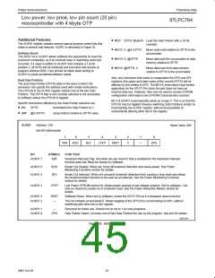
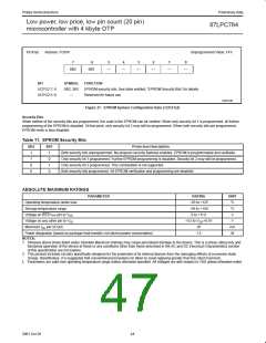
UCFG1
Address: FD00h
Unprogrammed Value: FFh
7
6
5
4
3
2
1
0
WDTE RPD
PRHI
BOV
CLKR FOSC2 FOSC1 FOSC0
BIT
SYMBOL
FUNCTION
UCFG1.7
WDTE
Watchdog timer enable. When programmed (0), disables the watchdog timer. The timer may
still be used to generate an interrupt.
UCFG1.6
RPD
Reset pin disable. When 1 disables the reset function of pin P1.5, allowing it to be used as an
input only port pin.
UCFG1.5
UCFG1.4
PRHI
BOV
Port reset high. When 1, ports reset to a high state. When 0, ports reset to a low state.
Brownout voltage select. When 1, the brownout detect voltage is 2.5V. When 0, the brownout
detect voltage is 3.8V. This is described in the Power Monitoring Functions section.
UCFG1.3
CLKR
Clock rate select. When 0, the CPU clock rate is divided by 2. This results in machine cycles
taking 12 CPU clocks to complete as in the standard 80C51. For full backward compatibility,
this division applies to peripheral timing as well.
UCFG1.2–0 FOSC2–FSOC0
CPU oscillator type select. See Oscillator section for additional information. Combinations
other than those shown below should not be used. They are reserved for future use.
FOSC2–FOSC0
1 1 1
Oscillator Configuration
External clock input on X1 (default setting for an unprogrammed part).
Internal RC oscillator, 6 MHz. For tolerance, see AC Electrical Characteristics table.
Low frequency crystal, 20 kHz to 100 kHz.
0 1 1
0 1 0
0 0 1
Medium frequency crystal or resonator, 100 kHz to 4 MHz.
High frequency crystal or resonator, 4 MHz to 20 MHz.
SU01477
0 0 0
Figure 36. EPROM System Configuration Byte 1 (UCFG1)
43
2001 Oct 26

 NXP [ NXP ]