Philips Semiconductors
Preliminary data
Low power, low price, low pin count (20 pin)
microcontroller with 4 kbyte OTP
87LPC764
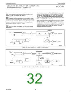
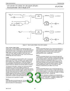
OSC/6
OSC/12
OR
C/T = 0
OVERFLOW
TL0
(8 BITS)
TF0
INTERRUPT
T0 PIN
CONTROL
C/T = 1
TR0
TOGGLE
GATE
T0 PIN
INT0 PIN
T0OE
TF1
OVERFLOW
TH0
(8 BITS)
OSC/6
OSC/12
OR
INTERRUPT
CONTROL
TOGGLE
TR1
T1 PIN
T1OE
SU01176
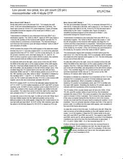
Figure 27. Timer/Counter 0 Mode 3 (Two 8-Bit Counters)
Mode 1
Timer Overflow Toggle Output
Timers 0 and 1 can be configured to automatically toggle a port
output whenever a timer overflow occurs. The same device pins that
are used for the T0 and T1 count inputs are also used for the timer
toggle outputs. This function is enabled by control bits T0OE and
T1OE in the P2M1 register, and apply to Timer 0 and Timer 1
respectively. The port outputs will be a logic 1 prior to the first timer
overflow when this mode is turned on.
10 bits are transmitted (through TxD) or received (through RxD): a
start bit (logical 0), 8 data bits (LSB first), and a stop bit (logical 1).
When data is received, the stop bit is stored in RB8 in Special
Function Register SCON. The baud rate is variable and is
determined by the Timer 1 overflow rate.
Mode 2
11 bits are transmitted (through TxD) or received (through RxD):
start bit (logical 0), 8 data bits (LSB first), a programmable 9th data
bit, and a stop bit (logical 1). When data is transmitted, the 9th data
bit (TB8 in SCON) can be assigned the value of 0 or 1. Or, for
example, the parity bit (P, in the PSW) could be moved into TB8.
When data is received, the 9th data bit goes into RB8 in Special
Function Register SCON, while the stop bit is ignored. The baud
rate is programmable to either 1/16 or 1/32 of the CPU clock
frequency, as determined by the SMOD1 bit in PCON.
UART
The 87LPC764 includes an enhanced 80C51 UART. The baud rate
source for the UART is timer 1 for modes 1 and 3, while the rate is
fixed in modes 0 and 2. Because CPU clocking is different on the
87LPC764 than on the standard 80C51, baud rate calculation is
somewhat different. Enhancements over the standard 80C51 UART
include Framing Error detection and automatic address recognition.
The serial port is full duplex, meaning it can transmit and receive
simultaneously. It is also receive-buffered, meaning it can
Mode 3
11 bits are transmitted (through TxD) or received (through RxD): a
start bit (logical 0), 8 data bits (LSB first), a programmable 9th data
bit, and a stop bit (logical 1). In fact, Mode 3 is the same as Mode 2
in all respects except baud rate. The baud rate in Mode 3 is variable
and is determined by the Timer 1 overflow rate.
commence reception of a second byte before a previously received
byte has been read from the SBUF register. However, if the first byte
still hasn’t been read by the time reception of the second byte is
complete, the first byte will be lost. The serial port receive and
transmit registers are both accessed through Special Function
Register SBUF. Writing to SBUF loads the transmit register, and
reading SBUF accesses a physically separate receive register.
In all four modes, transmission is initiated by any instruction that
uses SBUF as a destination register. Reception is initiated in Mode 0
by the condition RI = 0 and REN = 1. Reception is initiated in the
other modes by the incoming start bit if REN = 1.
The serial port can be operated in 4 modes:
Mode 0
Serial data enters and exits through RxD. TxD outputs the shift
clock. 8 bits are transmitted or received, LSB first. The baud rate is
fixed at 1/6 of the CPU clock frequency.
30
2001 Oct 26

 NXP [ NXP ]