Philips Semiconductors
Preliminary specification
80C51 8-bit microcontroller
8K/256 OTP, 8 channel 10 bit A/D, I2C, PWM,
capture/compare, high I/O, low voltage (2.7V–5.5V), low power
P87C552
V
DD
R
R
P
P
SDA
SCL
2
I
C bus
P1.7/SDA
P1.6/SCL
OTHER DEVICE WITH
2
OTHER DEVICE WITH
2
8XC554
I
C INTERFACE
I
C INTERFACE
SU00964
2
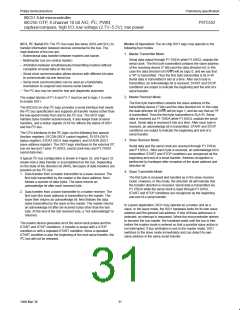
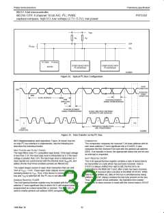
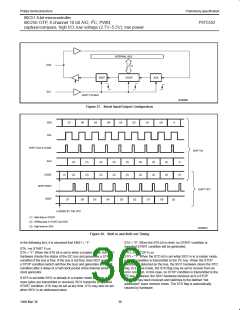
Figure 32. Typical I C Bus Configuration
STOP
CONDITION
SDA
REPEATED
START
CONDITION
MSB
SLAVE ADDRESS
R/W
DIRECTION
BIT
ACKNOWLEDGMENT
SIGNAL FROM RECEIVER
ACKNOWLEDGMENT
SIGNAL FROM RECEIVER
CLOCK LINE HELD LOW WHILE
INTERRUPTS ARE SERVICED
SCL
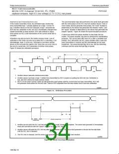
1
2
7
8
9
1
2
3–8
9
ACK
ACK
S
P/S
REPEATED IF MORE BYTES
ARE TRANSFERRED
START
CONDITION
SU00965
2
Figure 33. Data Transfer on the I C Bus
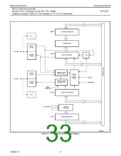
SIO1 Implementation and Operation: Figure 34 shows how the
on-chip I C bus interface is implemented, and the following text
COMPARATOR
2
The comparator compares the received 7-bit slave address with its
own slave address (7 most significant bits in S1ADR). It also
compares the first received 8-bit byte with the general call address
(00H). If an equality is found, the appropriate status bits are set and
an interrupt is requested.
describes the individual blocks.
INPUT FILTERS AND OUTPUT STAGES
2
The input filters have I C compatible input levels. If the input voltage
is less than 1.5V, the input logic level is interpreted as 0; if the input
voltage is greater than 3.0V, the input logic level is interpreted as 1.
SHIFT REGISTER, S1DAT
Input signals are synchronized with the internal clock (f
/4), and
This 8-bit special function register contains a byte of serial data to
be transmitted or a byte which has just been received. Data in
S1DAT is always shifted from right to left; the first bit to be
transmitted is the MSB (bit 7) and, after a byte has been received,
the first bit of received data is located at the MSB of S1DAT. While
data is being shifted out, data on the bus is simultaneously being
shifted in; S1DAT always contains the last byte present on the bus.
Thus, in the event of lost arbitration, the transition from master
transmitter to slave receiver is made with the correct data in S1DAT.
OSC
spikes shorter than three oscillator periods are filtered out.
The output stages consist of open drain transistors that can sink
3mA at V < 0.4V. These open drain outputs do not have
OUT
2
clamping diodes to V . Thus, if the device is connected to the I C
DD
2
bus and V is switched off, the I C bus is not affected.
DD
ADDRESS REGISTER, S1ADR
This 8-bit special function register may be loaded with the 7-bit slave
address (7 most significant bits) to which SIO1 will respond when
programmed as a slave transmitter or receiver. The LSB (GC) is
used to enable general call address (00H) recognition.
32
1999 Mar 30

 NXP [ NXP ]