Philips Semiconductors
Preliminary specification
80C51 8-bit microcontroller
8K/256 OTP, 8 channel 10 bit A/D, I2C, PWM,
capture/compare, high I/O, low voltage (2.7V–5.5V), low power
P87C552
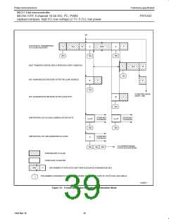
SERIAL CLOCK GENERATOR
read from and write to this 8-bit, directly addressable SFR while it is
not in the process of shifting a byte. This occurs when SIO1 is in a
defined state and the serial interrupt flag is set. Data in S1DAT
remains stable as long as SI is set. Data in S1DAT is always shifted
from right to left: the first bit to be transmitted is the MSB (bit 7), and,
after a byte has been received, the first bit of received data is
located at the MSB of S1DAT. While data is being shifted out, data
on the bus is simultaneously being shifted in; S1DAT always
contains the last data byte present on the bus. Thus, in the event of
lost arbitration, the transition from master transmitter to slave
receiver is made with the correct data in S1DAT.
This programmable clock pulse generator provides the SCL clock
pulses when SIO1 is in the master transmitter or master receiver
mode. It is switched off when SIO1 is in a slave mode. The
programmable output clock frequencies are: f
/120, f
/9600,
OSC
OSC
and the Timer 1 overflow rate divided by eight. The output clock
pulses have a 50% duty cycle unless the clock generator is
synchronized with other SCL clock sources as described above.
TIMING AND CONTROL
The timing and control logic generates the timing and control signals
for serial byte handling. This logic block provides the shift pulses for
S1DAT, enables the comparator, generates and detects start and
stop conditions, receives and transmits acknowledge bits, controls
the master and slave modes, contains interrupt request logic, and
7
6
5
4
3
2
1
0
S1DAT (DAH)
SD7
SD6
SD5
SD4
SD3
SD2
SD1
SD0
shift direction
2
monitors the I C bus status.
SD7 - SD0:
CONTROL REGISTER, S1CON
This 7-bit special function register is used by the microcontroller to
control the following SIO1 functions: start and restart of a serial
transfer, termination of a serial transfer, bit rate, address recognition,
and acknowledgment.
Eight bits to be transmitted or just received. A logic 1 in S1DAT
corresponds to a high level on the I C bus, and a logic 0
corresponds to a low level on the bus. Serial data shifts through
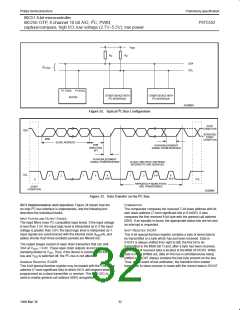
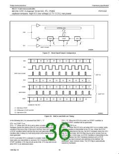
S1DAT from right to left. Figure 37 shows how data in S1DAT is
serially transferred to and from the SDA line.
2
STATUS DECODER AND STATUS REGISTER
The status decoder takes all of the internal status bits and
compresses them into a 5-bit code. This code is unique for each I C
S1DAT and the ACK flag form a 9-bit shift register which shifts in or
shifts out an 8-bit byte, followed by an acknowledge bit. The ACK
flag is controlled by the SIO1 hardware and cannot be accessed by
the CPU. Serial data is shifted through the ACK flag into S1DAT on
the rising edges of serial clock pulses on the SCL line. When a byte
has been shifted into S1DAT, the serial data is available in S1DAT,
and the acknowledge bit is returned by the control logic during the
ninth clock pulse. Serial data is shifted out from S1DAT via a buffer
(BSD7) on the falling edges of clock pulses on the SCL line.
2
bus status. The 5-bit code may be used to generate vector
addresses for fast processing of the various service routines. Each
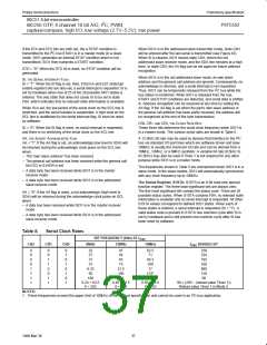
service routine processes a particular bus status. There are 26
possible bus states if all four modes of SIO1 are used. The 5-bit
status code is latched into the five most significant bits of the status
register when the serial interrupt flag is set (by hardware) and
remains stable until the interrupt flag is cleared by software. The
three least significant bits of the status register are always zero. If
the status code is used as a vector to service routines, then the
routines are displaced by eight address locations. Eight bytes of
code is sufficient for most of the service routines (see the software
example in this section).
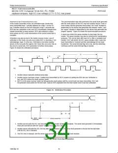
When the CPU writes to S1DAT, BSD7 is loaded with the content of
S1DAT.7, which is the first bit to be transmitted to the SDA line (see
Figure 38). After nine serial clock pulses, the eight bits in S1DAT will
have been transmitted to the SDA line, and the acknowledge bit will
be present in ACK. Note that the eight transmitted bits are shifted
back into S1DAT.
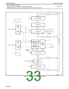
The Four SIO1 Special Function Registers: The microcontroller
interfaces to SIO1 via four special function registers. These four
SFRs (S1ADR, S1DAT, S1CON, and S1STA) are described
individually in the following sections.
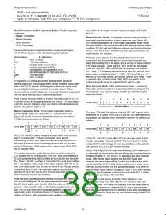
The Control Register, S1CON: The CPU can read from and write
to this 8-bit, directly addressable SFR. Two bits are affected by the
SIO1 hardware: the SI bit is set when a serial interrupt is requested,
and the STO bit is cleared when a STOP condition is present on the
The Address Register, S1ADR: The CPU can read from and write
to this 8-bit, directly addressable SFR. S1ADR is not affected by the
SIO1 hardware. The contents of this register are irrelevant when
SIO1 is in a master mode. In the slave modes, the seven most
significant bits must be loaded with the microcontroller’s own slave
address, and, if the least significant bit is set, the general call
address (00H) is recognized; otherwise it is ignored.
2
I C bus. The STO bit is also cleared when ENS1 = “0”.
7
6
5
4
3
2
1
0
S1CON (D8H) CR2
ENS1
STA
STO
SI
AA
CR1
CR0
ENS1, THE SIO1 ENABLE BIT
ENS1 = “0”: When ENS1 is “0”, the SDA and SCL outputs are in a
high impedance state. SDA and SCL input signals are ignored, SIO1
is in the “not addressed” slave state, and the STO bit in S1CON is
forced to “0”. No other bits are affected. P1.6 and P1.7 may be used
as open drain I/O ports.
7
6
5
4
3
2
1
0
S1ADR (DBH)
X
X
X
X
X
X
X
GC
own slave address
The most significant bit corresponds to the first bit received from the
ENS1 = “1”: When ENS1 is “1”, SIO1 is enabled. The P1.6 and P1.7
port latches must be set to logic 1.
2
I C bus after a start condition. A logic 1 in S1ADR corresponds to a
2
high level on the I C bus, and a logic 0 corresponds to a low level
ENS1 should not be used to temporarily release SIO1 from the I2C
bus since, when ENS1 is reset, the I2C bus status is lost. The AA
flag should be used instead (see description of the AA flag in the
following text).
on the bus.
The Data Register, S1DAT: S1DAT contains a byte of serial data to
be transmitted or a byte which has just been received. The CPU can
35
1999 Mar 30

 NXP [ NXP ]