P82B715
NXP Semiconductors
I2C-bus extender
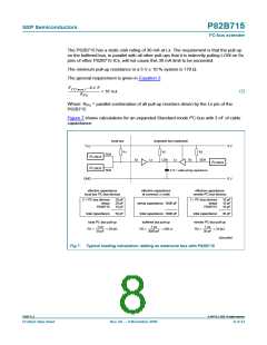
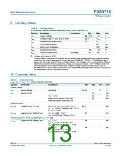
Figure 10 shows the I2C-bus waveforms from the long distance line as seen by the slave
on the P82B715 Sx/Sy I/O. Notice that the offset is small and the static levels remain
under 0.4 V. Coupling of SDA to SCL is negligible when SCL is LOW but slight
cross-coupling of SCL to SDA is visible when SDA is HIGH and therefore higher
impedance. The waveforms are very clean and will easily support all available I2C-bus
masters and slaves.
002aad819
7
voltage
(V)
5
SDA
3
SDA
SCL
SCL
SCL
SDA
1
SCL
−1
0
4
8
12
16
20
time (µs)
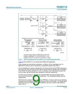
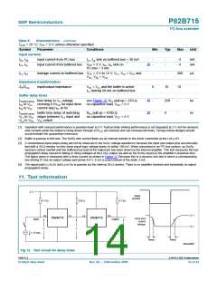
Fig 11. Clock and data signal output to a slave from Sx/Sy of a P82B96 replacing one of
the P82B715s
Figure 11 shows the waveforms on the Sx/Sy I/O as seen by the slave when a P82B96 is
substituted. P82B96 uses a static level offset on the slave side to isolate noise and
loadings on either side of this device. The nominal offset is 0.8 V and that VOL may create
worst-case design tolerance problems with slave devices that do not use I2C-bus
switching levels, for example TTL levels. It also precludes operation with other bus buffers
using special non-compliant I2C-bus levels.
The P82B96 does not actually interfere with the operation of compliant I2C-bus devices
down to at least 2.7 V supply or even with TTL devices (that switch around 1.4 V). It only
causes a theoretical worst case design tolerance problem because TTL devices have a
worst case 0.8 V requirement. A TTL designer must center the actual switch point
between the two specified limits, 0.8 V and 2.1 V, so in reality it cannot ever approach the
problem 0.8 V theoretical limit.
The PCA9600 is an improved version of the P82B96 offering 1 MHz operation and lower,
more closely controlled VOL on the Sx and Sy pins.
P82B715_8
© NXP B.V. 2009. All rights reserved.
Product data sheet
Rev. 08 — 9 November 2009
12 of 23

 NXP [ NXP ]