P82B715
NXP Semiconductors
I2C-bus extender
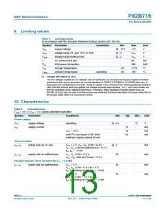
Table 5.
Characteristics …continued
Tamb = 25 °C; VCC = 5 V; unless otherwise specified.
Symbol
Parameter
Conditions
Min
Typ
Max
Unit
Input currents
ISx, ISy
ILx, ILy
input current from I2C-bus
ILx, ILy sink on buffered bus = 30 mA
-
-
-
-
−3
−3
mA
mA
[2]
input current from buffered bus VCC > 3 V; ISx, ISy sink on
I2C-bus = 3 mA
ILx, ILy
leakage current on buffered bus VCC = 3 V to 12 V; VLx, VLy = VCC and
-
-
200
13
µA
VSx, VSy = VCC
Impedance transformation
Zin/Zout
input/output impedance
VSx < VLx and the buffer is active;
Lx sinking 30 mA on buffered bus
8
10
I
Buffer delay times
[3]
[4]
trise/fall delay time delay to VLx voltage
see Figure 12; RLx pull-up = 270 Ω;
no capacitive load; VCC = 5 V
-
-
250
0
-
-
ns
ns
ISx to VLx
ISy to VLy
crossing 0.5VCC for input drive
current step ISx at Sx
trise/fall delay buffer time delay of switching
VLx to VSx edges between VLx input and
RSx pull-up = 4700 Ω;
no capacitive load; VCC = 5 V
VLy to VSy
VSx output
[1] Operation with reduced performance is possible down to 3 V. Typical static sinking performance is not degraded at 3 V, but the dynamic
sink currents while the output is being driven through 0.5VCC are reduced and can increase fall times. Timing-critical designs should
accommodate the guaranteed minimums.
[2] Buffer is passive in this test. The Sx/Sy sink current flows via an internal resistor to the driver connected at the Lx/Ly I/O.
[3] A conventional input-output delay will not be observed in the Sx/Lx voltage waveforms because the input and output pins are internally
tied with a 30 Ω resistor so they show equal logic voltage levels, to within 100 mV. When connected in an I2C-bus system, an Sx/Sy
input pin cannot rise/fall until the buffered bus load at the output pin has been driven by the internal amplifier. This test measures the bus
propagation delay caused to falling or rising voltages at the Lx/Ly output (as well as the Sx/Sy input) by the amplifier’s response time.
The figure given is measured with a drive current as shown in Figure 12. Because this is a dynamic bus test in which a corresponding
bus driving IC has an output voltage well above 0.4 V, 6 mA is used instead of the static 3 mA.
[4] The signal path Lx to Sx and Ly to Sy is passive via the internal 30 Ω resistor. There is no amplifier involved and essentially no signal
propagation delay.
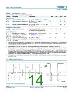
11. Test information
5 V
input
current
4.7 kΩ
270 Ω
4.7 kΩ
5 V
0 V
Sx
V
Lx
Lx
Sx
P82B715
P82B715
input and
output
voltage
input
output
V
V
I = 6 mA
t
t
delay
delay
002aad693
Fig 12. Test circuit for delay times
P82B715_8
© NXP B.V. 2009. All rights reserved.
Product data sheet
Rev. 08 — 9 November 2009
14 of 23

 NXP [ NXP ]