Philips Semiconductors Linear Products
Product specification
Tone decoder/phase-locked loop
NE/SE567
cause supply voltage fluctuations which could, for example, shift the
detection band of narrow-band systems sufficiently to cause
momentary loss of lock. The result is a low-frequency oscillation into
and out of lock. Such effects can be prevented by supplying heavy
load currents from a separate supply or increasing the supply filter
capacitor.
V+
R
1
567
567 1
C
3
R
C
3
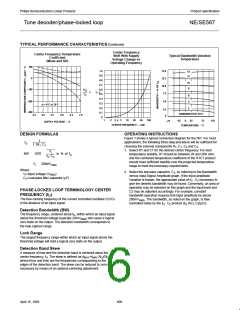
SPEED OF OPERATION
Minimum lock-up time is related to the natural frequency of the loop.
The lower it is, the longer becomes the turn-on transient. Thus,
DECREASE
SENSITIVITY
INCREASE
SENSITIVITY
maximum operating speed is obtained when C is at a minimum.
2
V+
When the signal is first applied, the phase may be such as to initially
drive the controlled oscillator away from the incoming frequency
rather than toward it. Under this condition, which is of course
unpredictable, the lock-up transient is at its worst and the theoretical
minimum lock-up time is not achievable. We must simply wait for the
transient to die out.
DECREASE
SENSITIVITY
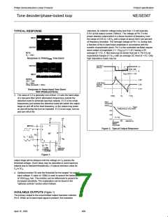
R
A
R
2.5k
B
567 1
50k
C
INCREASE
SENSITIVITY
3
R
C
1.0k
SILICON
The following expressions give the values of C and C which allow
2
3
DIODES FOR
TEMPERATURE
COMPENSATION
(OPTIONAL)
highest operating speeds for various band center frequencies. The
minimum rate at which digital information may be detected without
information loss due to the turn-on transient or output chatter is
about 10 cycles per bit, corresponding to an information transfer rate
Figure 3. Sensitivity Adjust
of f /10 baud.
O
connected to pin 6 without affecting the CCO duty cycle or
temperature stability.
V+
V+
V+
V+
R
A
R
C
L
200 TO 1k
R
L
OPERATING PRECAUTIONS
A brief review of the following precautions will help the user achieve
the high level of performance of which the 567 is capable.
8
8
567
1
567
1
R
10k
R
L
f
R
f
f
1
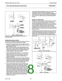
1. Operation in the high input level mode (above 200mV) will free
the user from bandwidth variations due to changes in the in-band
signal amplitude. The input
stage is now limiting, however, so that out-band signals or high
noise levels can cause an apparent bandwidth reduction as the
inband signal is suppressed. Also, the limiting action will create
in-band components from sub-harmonic signals, so the 567
10k
C
3
8
R *
f
567
C
3
10k
R
A
200 TO
1k
*OPTIONAL - PERMITS
LOWER VALUE OF C
f
Figure 4. Chatter Prevention
becomes sensitive to signals at f /3, f /5, etc.
O
O
V+
2. The 567 will lock onto signals near (2n+1) f , and will give an
O
output for signals near (4n+1) f where n=0, 1, 2, etc. Thus,
O
signals at 5f and 9f can cause an unwanted output. If such
O
O
R
signals are anticipated, they should be attenuated before
reaching the 567 input.
3. Maximum immunity from noise and out-band signals is afforded
2
567 2
567
C
2
R
C
2
LOWERS f
RAISES f
O
O
in the low input level (below 200mV
) and reduced bandwidth
RMS
operating mode. However, decreased loop damping causes the
worst-case lock-up time to increase, as shown by the Greatest
Number of Cycles Before Output vs Bandwidth graph.
V+
LOWERS f
O
R
A
R
2.5k
4. Due to the high switching speeds (20ns) associated with 567
operation, care should be taken in lead routing. Lead lengths
should be kept to a minimum. The power supply should be
adequately bypassed close to the 567 with a 0.01µF or greater
capacitor; grounding paths should be carefully chosen to avoid
ground loops and unwanted voltage variations. Another factor
which must be considered is the effect of load energization on
the power supply. For example, an incandescent lamp typically
draws 10 times rated current at turn-on. This can be somewhat
greater when the output stage is made less sensitive, rejection of
third harmonics or in-band harmonics (of lower frequency
signals) is also improved.
B
567 1
50k
C
2
R
C
RAISES f
O
RAISES f
O
1.0k
SILICON
DIODES FOR
TEMPERATURE
COMPENSATION
(OPTIONAL)
Figure 5. Skew Adjust
410
April 15, 1992

 NXP [ NXP ]