Philips Semiconductors Linear Products
Product specification
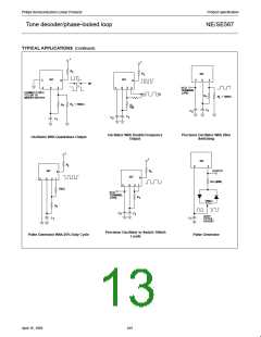
Tone decoder/phase-locked loop
NE/SE567
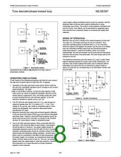
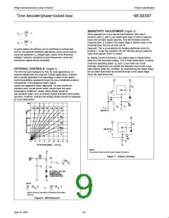
SENSITIVITY ADJUSTMENT (Figure 3)
130
fO
C2
C3
+
+
F
F
When operated as a very narrow-band detector (less than 8
percent), both C and C are made quite large in order to improve
2
3
noise and out-band signal rejection. This will inevitably slow the
response time. If, however, the output stage is biased closer to the
threshold level, the turn-on time can be
260
fO
improved. This is accomplished by drawing additional current to
terminal 1. Under this condition, the 567 will also give an output for
lower-level signals (10mV or lower).
In cases where turn-off time can be sacrificed to achieve fast
turn-on, the optional sensitivity adjustment circuit can be used to
move the quiescent C voltage lower (closer to the threshold
3
voltage). However, sensitivity to beat frequencies, noise and
extraneous signals will be increased.
By adding current to terminal 1, the output stage is biased further
away from the threshold voltage. This is most useful when, to obtain
maximum operating speed, C and C are made very small.
2
3
Normally, frequencies just outside the detection band could cause
false outputs under this condition. By desensitizing the output stage,
the out-band beat notes do not feed through to the output stage.
Since the input level must
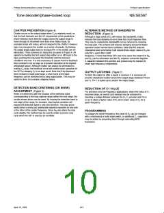
OPTIONAL CONTROLS (Figure 3)
The 567 has been designed so that, for most applications, no
external adjustments are required. Certain applications, however,
will be greatly facilitated if full advantage is taken of the added
control possibilities available through the use of additional external
components. In the diagrams given, typical
V+
V+
values are suggested where applicable. For best results the
resistors used, except where noted, should have the same
temperature coefficient. Ideally, silicon diodes would be
low-resistivity types, such as forward-biased transistor base-emitter
junctions. However, ordinary low-voltage diodes should be adequate
for most applications.
R
L
567
1
8
R
A
10k
250
R
f
20k
C
C
3
A
0.5k 0.9k 1.4k 1.9k 2.5k 3.2k 4.0k
200
UNLATCH
10k
V+
150
V+
20k
R
L
100
567
8
100k
UNLATCH
1
50
R
R
20k
f
0
C
3
0
2
4
6
8
10
12
14
16
DETECTION BAND — % OF f
O
NOTE:
prevents latch-up when power supply is turned on.
V+
C
A
R
A
Figure 7. Output Latching
50k
R
B
PIN 2
567
R
R
B
C
R
R
+ R
A
R
B
C
C
2
R
C
OPTIONAL SILICON
DIODES FOR
TEMPERATURE
COMPENSATION
NOTE:
130 10k
R
1300 10k
R
C
2
f
R
f
R
O
O
Adjust control for symmetry of detection band edges
about f
.
O
Figure 6. BW Reduction
411
April 15, 1992

 NXP [ NXP ]