Philips Semiconductors Linear Products
Product specification
Tone decoder/phase-locked loop
NE/SE567
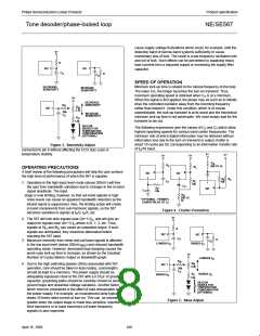
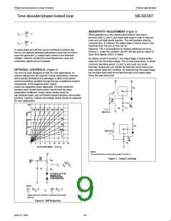
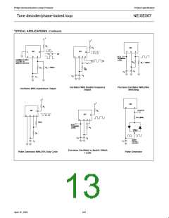
CHATTER PREVENTION (Figure 4)
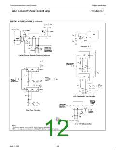
ALTERNATE METHOD OF BANDWIDTH
Chatter occurs in the output stage when C is relatively small, so
REDUCTION (Figure 6)
3
that the lock transient and the AC components at the quadrature
phase detector (lock detector) output cause the output stage to
move through its threshold more than once. Many loads, for
example lamps and relays, will not respond to the chatter. However,
logic may recognize the chatter as a series of outputs. By feeding
the output stage output back to its input (Pin 1) the chatter can be
eliminated. Three schemes for doing this are given in Figure 4. All
operate by feeding the first output step (either on or off) back to the
input, pushing the input past the threshold until the transient
conditions are over. It is only necessary to assure that the feedback
time constant is not so large as to prevent operation at the highest
anticipated speed. Although chatter can always be eliminated by
Although a large value of C will reduce the bandwidth, it also
2
reduces the loop damping so as to slow the circuit response time.
This may be undesirable. Bandwidth can be reduced by reducing
the loop gain. This scheme will improve damping and permit faster
operation under narrow-band conditions. Note that the reduced
impedance level at terminal 2 will require that a larger value of C be
used for a given filter cutoff
2
frequency. If more than three 567s are to be used, the network of R
B
and R can be eliminated and the R resistors connected together.
C
A
A capacitor between this junction and ground may be required to
shunt high frequency components.
making C large, the feedback circuit will enable faster operation of
3
the 567 by allowing C to be kept small. Note that if the feedback
3
OUTPUT LATCHING (Figure 7)
time constant is made quite large, a short burst at the input
frequency can be stretched into a long output pulse. This may be
useful to drive, for example, stepping relays.
To latch the output on after a signal is received, it is necessary to
provide a feedback resistor around the output stage (between Pins 8
and 1). Pin 1 is pulled up to unlatch the output stage.
DETECTION BAND CENTERING (OR SKEW)
ADJUSTMENT (Figure 5)
REDUCTION OF C1 VALUE
For precision very low-frequency applications, where the value of C
becomes large, an overall cost savings may be achieved by
1
When it is desired to alter the location of the detection band
(corresponding to the loop capture range) within the lock range, the
circuits shown above can be used. By moving the detection band to
one edge of the range, for example, input signal variations will
expand the detection band in only one direction. This may prove
useful when a strong but undesirable signal is expected on one side
inserting a voltage-follower between the R C junction and Pin 6,
1
1
so as to allow a higher value of R and a lower value of C for a
1
1
given frequency.
or the other of the center frequency. Since R also alters the duty
cycle slightly, this method may be used to obtain a precise duty
cycle when the 567 is used as an oscillator.
B
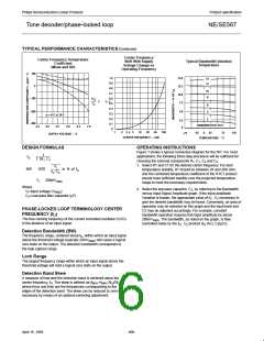
PROGRAMMING
To change the center frequency, the value of R can be changed
1
with a mechanical or solid state switch, or additional C capacitors
1
may be added by grounding them through saturating NPN
transistors.
412
April 15, 1992

 NXP [ NXP ]