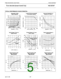
Philips Semiconductors Linear Products
Product specification
Tone decoder/phase-locked loop
NE/SE567
DC ELECTRICAL CHARACTERISTICS
V +=5.0V; T =25°C, unless otherwise specified.
A
SYM-
PARAMETER
BOL
TEST CONDITIONS
SE567
Typ
NE567
Typ
UNIT
Max
Min
Max
Min
Center frequency1
f
f
Highest center frequency
500
35 ±140
35 ±60
0
500
35 ±140
35 ±60
0
kHz
O
O
2
Center frequency stability
-55 to +125°C
0 to +70°C
ppm/°C
ppm/°C
f
Center frequency distribution
-10
+10
1
-10
+10
2
%
1
O
O
fO + 100kHz +
1.1R1C1
f
Center frequency shift with supply
voltage
0.5
14
0.7
14
%/V
1
fO + 100kHz +
1.1R1C1
Detection bandwidth
BW
Largest detection bandwidth
12
16
4
10
18
6
% of f
% of f
1
O
fO + 100kHz +
1.1R1C1
BW
BW
Largest detection bandwidth skew
Largest detection bandwidth—
variation with temperature
2
3
O
V =300mV
±0.1
±0.1
%/°C
I
RMS
BW
Largest detection bandwidth—
variation with supply voltage
V =300mV
±2
±2
%/V
I
RMS
Input
R
Input resistance
15
10
20
20
15
+6
25
25
15
10
20
20
15
+6
25
25
kΩ
IN
4
V
I
Smallest detectable input voltage
I =100mA, f =f
mV
L
I
O
RMS
RMS
4
Largest no-output input voltage
I =100mA, f =f
mV
L
I
O
Greatest simultaneous out-band
signal-to-in-band signal ratio
dB
Minimum input signal to wide-band
noise ratio
B =140kHz
n
-6
-6
dB
Output
Fastest on-off cycling rate
“1” output leakage current
“0” output voltage
f /20
f /20
O
O
V =15V
0.01
0.2
0.6
30
25
0.4
1.0
0.01
0.2
0.6
30
25
0.4
1.0
µA
V
8
I =30mA
L
I =100mA
L
V
3
t
t
Output fall time
R =50Ω
L
ns
ns
F
3
Output rise time
R =50Ω
L
150
150
R
General
V
Operating voltage range
Supply current quiescent
Supply current—activated
Quiescent power dissipation
4.75
9.0
8
4.75
9.0
10
15
V
CC
6
7
mA
mA
mW
R =20kΩ
L
11
30
13
12
35
t
PD
NOTES:
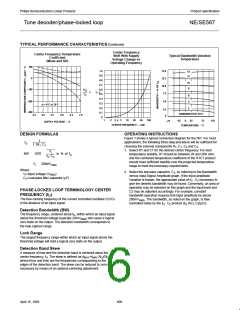
1. Frequency determining resistor R should be between 2 and 20kΩ
1
2. Applicable over 4.75V to 5.75V. See graphs for more detailed information.
3. Pin 8 to Pin 1 feedback R network selected to eliminate pulsing during turn-on and turn-off.
L
4. With R =130kΩ from Pin 1 to V+. See Figure 1.
2
406
April 15, 1992

 NXP [ NXP ]