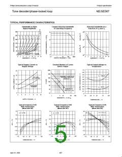
Philips Semiconductors Linear Products
Product specification
Tone decoder/phase-locked loop
NE/SE567
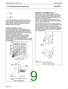
saturates; its collector voltage being less than 1.0 volt (typically
0.6V) at full output current (100mA). The voltage at Pin 2 is the
phase detector output which is a linear function of frequency over
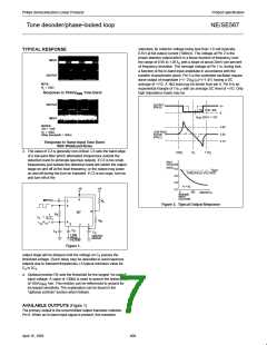
TYPICAL RESPONSE
INPUT
the range of 0.95 to 1.05 f with a slope of about 20mV per percent
O
of frequency deviation. The average voltage at Pin 1 is, during lock,
a function of the in-band input amplitude in accordance with the
transfer characteristic given. Pin 5 is the controlled oscillator square
OUTPUT
NOTE:
wave output of magnitude (+V -2V ) (+V-1.4V) having a DC
BE
average of +V/2. A 1kΩ load may be driven from pin 5. Pin 6 is an
R
= 100Ω
L
exponential triangle of 1V
with an average DC level of +V/2. Only
P-P
Response to 100mV
Tone Burst
high impedance loads may be
RMS
OUTPUT
OUTPUT
(PIN 8)
V+
7% 14% BW
0
V
(SAT) < 1.0V
CE
INPUT
NOTES:
S/N = –6dB
3.9V
3.8V
3.7V
LOW PASS
FILTER
(PIN 2)
R
= 100Ω
L
Noise Bandwidth = 140Hz
Response to Same Input Tone Burst
With Wideband Noise
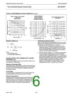
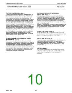
3. The value of C3 is generally non-critical. C3 sets the band edge
of a low-pass filter which attenuates frequencies outside the
detection band to eliminate spurious outputs. If C3 is too small,
frequencies just outside the detection band will switch the output
stage on and off at the beat frequency, or the output may pulse
on and off during the turn-on transient. If C3 is too large, turn-on
and turn-off of the
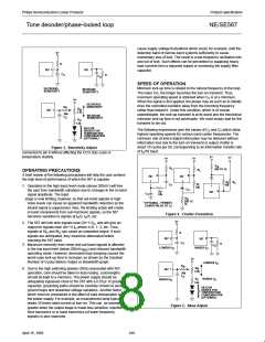
0.9f
O
f
1.1f
O
O
PIN 1
VOLTAGE
(AVG)
4.0
V
REF
THRESHOLD VOLTAGE
3.5
3.0
f
= f
O
1
+V
4
+V
2.5
0
100
200mVrms
IN-BAND
INPUT
VOLTAGE
INPUT
R
3
5
L
Figure 2. Typical Output Response
8
567
R
1
1
f
+
O
R
C
1
1
R
2
6
2
7
1
C
2
C
1
C
3
LOW
OUTPUT
FILTER
PASS
FILTER
Figure 1.
output stage will be delayed until the voltage on C passes the
3
threshold voltage. (Such delay may be desirable to avoid spurious
outputs due to transient frequencies.) A typical minimum value for
C is 2C .
3
2
4. Optional resistor R2 sets the threshold for the largest “no output”
input voltage. A value of 130kΩ is used to assure the tested limit
of 10mV
min. This resistor can be referenced to ground for
RMS
increased sensitivity. The explanation can be found in the
“optional controls” section which follows.
AVAILABLE OUTPUTS (Figure 1)
The primary output is the uncommitted output transistor collector,
Pin 8. When an in-band input signal is present, this transistor
409
April 15, 1992

 NXP [ NXP ]