ISP1362
Single-chip USB OTG controller
Philips Semiconductors
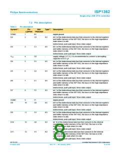
Table 2:
Symbol[1]
Pin description…continued
Pin Ball
LQFP64 TFBGA64
Type[2] Description
AGND
VCC
51
A8
B7
-
-
analog ground; used for OTG ATX
52
supply voltage (3.3 V); it is recommended to connect a decoupling
capacitor of 0.01 µF
CP_CAP1
CP_CAP2
VBUS
53
54
55
A7
B6
A6
AI/O
AI/O
I/O
charge pump capacitor pin 1; low ESR; see Section 11.6
charge pump capacitor pin 2; low ESR; see Section 11.6
analog input and output
OTG mode — built-in charge pump output or VBUS voltage
comparators input; connect to pin VBUS of the OTG connector
DC mode — input as VBUS sensing; connect to pin VBUS of the
upstream connector
HC mode — not used; leave open
VDD_5V
56
B5
I
supply reference voltage (5 V); to be used together with built-in
overcurrent circuit; when built-in overcurrent circuit is not in use, this
pin can be tied to VCC; it is recommended to connect a decoupling
capacitor of 0.01 µF
DGND
VCC
57
58
A5
B4
-
-
digital ground
supply voltage (3.3 V); it is recommended to connect a decoupling
capacitor of 0.01 µF
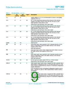
TEST1
TEST2
A0
59
60
61
62
A4
B3
A3
B2
I/O
for test input and output, pulled to GND by a 10 kΩ resistor
bidirectional, push-pull input, three-state output
for test input and output, pulled to GND by a 10 kΩ resistor
bidirectional, push-pull input, three-state output
command or data phase
I/O
I
I
input
A1
LOW — PIO bus of the HC is selected
HIGH — PIO bus of the DC is selected
input
D0
D1
63
64
A2
A1
I/O
I/O
bit 0 of the bidirectional data bus that connects to the internal registers
and buffer memory of the ISP1362; the bus is in the high-impedance
state when it is idle
bidirectional, push-pull input, three-state output
bit 1 of the bidirectional data bus that connects to the internal registers
and buffer memory of the ISP1362; the bus is in the high-impedance
state when it is idle
bidirectional, push-pull input, three-state output
[1] Symbol names with an overscore (for example, NAME) represent active LOW signals.
[2] All I/O pads are 5 V tolerant.
[3] In the OTG mode, this pin is pulled down by an internal resistor.
9397 750 12337
© Koninklijke Philips Electronics N.V. 2004. All rights reserved.
Product data
Rev. 03 — 06 January 2004
12 of 150

 NXP [ NXP ]