Philips Semiconductors
Product specification
2-input EXCLUSIVE-OR gate
74AHC1G86; 74AHCT1G86
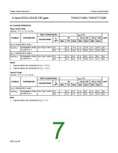
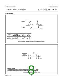
AC WAVEFORMS
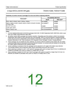
handbook, halfpage
A, B input
V
M
t
t
PHL
PLH
V
Y output
M
MNA041
VI INPUT
VM
VM
FAMILY
REQUIREMENTS INPUT OUTPUT
AHC1G
GND to VCC 50% VCC 50% VCC
1.5 V 50% VCC
AHCT1G GND to 3.0 V
Fig.5 The input (A and B) to output (Y) propagation delays.
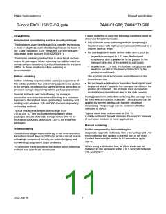
V
handbook, halfpage
CC
V
V
O
I
PULSE
GENERATOR
D.U.T.
C
50 pF
R
L
T
MNA034
Definitions for test circuit:
CL = load capacitance including jig and probe capacitance (see “AC characteristics” for values).
RT = termination resistance should be equal to the output impedance Zo of the pulse generator.
Fig.6 Load circuitry for switching times.
8
2002 Jun 06

 NXP [ NXP ]