Philips Semiconductors
Product specification
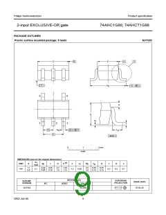
2-input EXCLUSIVE-OR gate
74AHC1G86; 74AHCT1G86
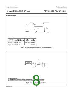
handbook, halfpage
B
handbook, halfpage
1
2
= 1
4
Y
MNA039
A
MNA040
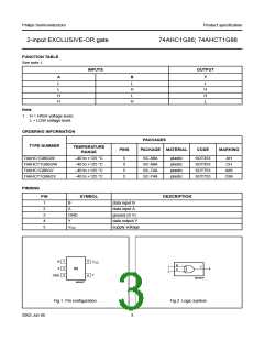
Fig.3 IEC logic symbol.
Fig.4 Logic diagram.
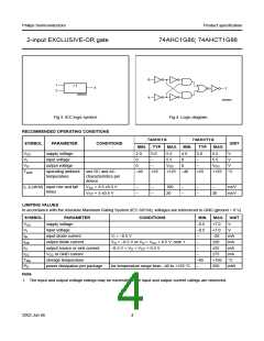
RECOMMENDED OPERATING CONDITIONS
74AHC1G
TYP. MAX. MIN.
74AHCT1G
TYP. MAX.
SYMBOL
PARAMETER
CONDITIONS
UNIT
MIN.
2.0
VCC
VI
supply voltage
input voltage
output voltage
5.0
−
5.5
5.5
VCC
4.5
0
5.0
−
5.5
5.5
VCC
V
0
V
V
VO
0
−
0
−
Tamb
operating ambient
temperature
see DC and AC
characteristics per
device
−40
+25
+125 −40
+25
+125 °C
tr, tf (∆t/∆f) input rise and fall
VCC = 3.3 ±0.3 V
−
−
−
−
100
20
−
−
−
−
−
ns/V
ns/V
times
VCC = 5 ±0.5 V
20
LIMITING VALUES
In accordance with the Absolute Maximum Rating System (IEC 60134); voltages are referenced to GND (ground = 0 V).
SYMBOL
PARAMETER
supply voltage
CONDITIONS
MIN. MAX. UNIT
VCC
VI
−0.5
−0.5
−
+7.0
+7.0
−20
±20
±25
±75
V
input voltage
V
IIK
input diode current
VI < −0.5 V
mA
mA
mA
mA
IOK
IO
output diode current
output source or sink current
VCC or GND current
storage temperature
power dissipation per package
VO < −0.5 V or VO > VCC + 0.5 V; note 1
−0.5 V < VO < VCC + 0.5 V
−
−
ICC
Tstg
PD
−
−65
−
+150 °C
250 mW
for temperature range from −40 to +125 °C
Note
1. The input and output voltage ratings may be exceeded if the input and output current ratings are observed.
2002 Jun 06
4

 NXP [ NXP ]