Philips Semiconductors
Product specification
2-input EXCLUSIVE-OR gate
74AHC1G86; 74AHCT1G86
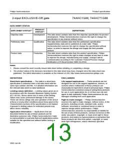
Suitability of surface mount IC packages for wave and reflow soldering methods
SOLDERING METHOD
WAVE
REFLOW(2)
not suitable suitable
PACKAGE(1)
BGA, LBGA, LFBGA, SQFP, TFBGA, VFBGA
HBCC, HBGA, HLQFP, HSQFP, HSOP, HTQFP, HTSSOP, HVQFN, not suitable(3)
HVSON, SMS
suitable
PLCC(4), SO, SOJ
LQFP, QFP, TQFP
SSOP, TSSOP, VSO
suitable
suitable
not recommended(4)(5) suitable
not recommended(6)
suitable
Notes
1. For more detailed information on the BGA packages refer to the “(LF)BGA Application Note” (AN01026); order a copy
from your Philips Semiconductors sales office.
2. All surface mount (SMD) packages are moisture sensitive. Depending upon the moisture content, the maximum
temperature (with respect to time) and body size of the package, there is a risk that internal or external package
cracks may occur due to vaporization of the moisture in them (the so called popcorn effect). For details, refer to the
Drypack information in the “Data Handbook IC26; Integrated Circuit Packages; Section: Packing Methods”.
3. These packages are not suitable for wave soldering. On versions with the heatsink on the bottom side, the solder
cannot penetrate between the printed-circuit board and the heatsink. On versions with the heatsink on the top side,
the solder might be deposited on the heatsink surface.
4. If wave soldering is considered, then the package must be placed at a 45° angle to the solder wave direction.
The package footprint must incorporate solder thieves downstream and at the side corners.
5. Wave soldering is suitable for LQFP, TQFP and QFP packages with a pitch (e) larger than 0.8 mm; it is definitely not
suitable for packages with a pitch (e) equal to or smaller than 0.65 mm.
6. Wave soldering is suitable for SSOP and TSSOP packages with a pitch (e) equal to or larger than 0.65 mm; it is
definitely not suitable for packages with a pitch (e) equal to or smaller than 0.5 mm.
2002 Jun 06
12

 NXP [ NXP ]