OXCB950
OXFORD SEMICONDUCTOR LTD.
950 mode:
950 mode:
Setting ACR[5]=1 enables 950-mode trigger levels set
using the TTL register (see section 7.11.4), FCR[5:4] are
ignored.
In similar fashion to for transmitter trigger levels, setting
ACR[5]=1 enables 950-mode receiver trigger levels.
FCR[7:6] are ignored.
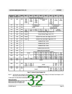
RHR trigger levels
FCR
[7:6]
Mode
550
Ext. 550 / 750
650
FIFO Size 16
FCR[7:6]: Compatible Trigger levels
L1
L2
n/a
n/a
n/a
LF1IFO SizeL1228
FLIF1O SizeL1228
00
01
10
11
1
1
1
1
1
1
16
32
1
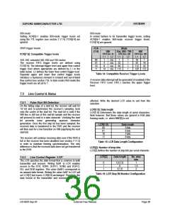
450, 550, extended 550, 650 and 750 modes:
The receiver FIFO trigger levels are defined using
FCR[7:6]. The interrupt trigger level and upper flow control
trigger level where appropriate are defined by L1 in the
table below. L2 defines the lower flow control trigger level.
Separate upper and lower flow control trigger levels
introduce a hysteresis element in in-band and out-of-band
flow control (see section 7.9). In Byte mode (450 mode) the
trigger levels are all set to 1.
4
32
64
16
32
8
112
14
n/a 112
120 112
Table 14: Compatible Receiver Trigger Levels
A receiver data interrupt will be generated (if enabled) if the
Receiver FIFO Level (‘RFL’) reaches the upper trigger
level.
7.5 Line Control & Status
7.5.1 False Start Bit Detection
affected. Write the desired LCR value to exit from this
selection.
On the falling edge of a start bit, the receiver will wait for
1/2 bit and re-synchronise the receiver’s sampling clock
onto the centre of the start bit. The start bit is valid if the
SIN line is still low at this mid-bit sample and the receiver
will proceed to read in a data character. Verifying the start
bit prevents noise generating spurious character
generation. Once the first stop bit has been sampled, the
received data is transferred to the RHR and the receiver
will then wait for a low transition on SIN (signifying the next
start bit).
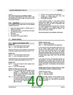
LCR[1:0]: Data length
LCR[1:0] Determines the data length of serial characters.
Note however, that these values are ignored in 9-bit data
framing mode, i.e. when NMR[0] is set.
LCR[1:0]
Data length
5 bits
00
01
10
11
6 bits
7 bits
8 bits
The receiver will continue receiving data even if the RHR is
full or the receiver has been disabled (see section 7.11.3)
in order to maintain framing synchronisation. The only
difference is that the received data does not get transferred
to the RHR.
Table 15: LCR Data Length Configuration
LCR[2]: Number of stop bits
LCR[2] defines the number of stop bits per serial character.
LCR[2]
Data length
No. stop
7.5.2 Line Control Register ‘LCR’
bits
1
The LCR specifies the data format that is common to both
transmitter and receiver. Writing 0xBF to LCR enables
access to the EFR, XON1, XOFF1, XON2 and XOFF2,
DLL and DLM registers. This value (0xBF) corresponds to
an unused data format. Writing the value 0xBF to LCR will
set LCR[7] but leaves LCR[6:0] unchanged. Therefore, the
data format of the transmitter and receiver data is not
0
1
1
5,6,7,8
5
1.5
2
6,7,8
Table 16: LCR Stop Bit Number Configuration
DS-0033 Sep 05
External-Free Release
Page 36

 OXFORD [ OXFORD SEMICONDUCTOR ]